
GaN Template (gallium nitride template)
UNIELECTRON ’s GaN Template consists of crystalline layers of gallium nitride (GaN), aluminum nitride (AlN), aluminum gallium nitride (AlGaN) and indium gallium nitride (InGaN), which are epilayer on sapphire and electronic grade for fabrication as MOS-based devices. UNIELECTRON ’s Gallium Nitride Template Products enable 20-50% shorter epitaxy cycle times and higher quality epitaxial device layers, with better structural quality and higher thermal conductivity,which can improve devices in the cost, yield, and performance.
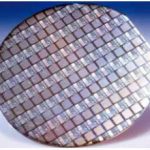
2″(50.8mm) GaN Templates Epitaxy on Sapphire Substrates
| Item | PAM-2inch-GaNT-N | PAM-2inch-GaNT-SI |
| Conduction Type | N-type | Semi-insulating |
| Dopant | Si doped or low doped | Fe doped |
| Size | 2″(50mm) dia. | |
| Thickness | 4um,20um,30um,50um,100um | 30um,90um |
| Orientation | C-axis(0001)+/-1° | |
| Resistivity(300K) | <0.05Ω·cm | >1×10⁶Ω·cm |
| Dislocation Density | <1x108cm-2 | |
| Substrate Structure | GaN on Sapphire(0001) | |
| Surface Finish | Single or Double Side Polished,epi-ready | |
| Usable Area | ≥ 90 % | |
2″ (50.8mm)GaN Templates Epitaxy on Sapphire Substrates
| Item | PAM-GaNT-P | |
| Conduction Type | P-type | |
| Dopant | Mg doped | |
| Size | 2″(50mm) dia. | |
| Thickness | 5um,20um,30um,50um,100um | |
| Orientation | C-axis(0001)+/-1° | |
| Resistivity(300K) | <1Ω·cm or custom | |
| Dopant Concentration | 1E17(cm-3) or custom | |
| Substrate Structure | GaN on Sapphire(0001) | |
| Surface Finish | Single or Double Side Polished,epi-ready | |
| Usable Area | ≥ 90 % | |
3″(76.2mm)GaN Templates Epitaxy on Sapphire Substrates
| Item | PAM-3inch-GaNT-N |
| Conduction Type | N-type |
| Dopant | Si doped |
| Exclusion Zone: | 5mm from outer diameter |
| Thickness: | 20um,30um |
| Dislocation density | < 1x108cm-2 |
| Sheet resistance (300K): | <0.05Ω·cm |
| Substrate: | sapphire |
| Orientation : | C-plane |
| Sapphire thickness: | 430um |
| Polishing: | Single side Polished,epi-ready, with atomic steps. |
| Backside coating: | (custom)high quality Titanium coating, thickness > 0.4 μm |
| Packing: | Individually packed under argon |
| Atmosphere vacuum sealed in class 100 clean room. |
3″(76.2mm)GaN Templates Epitaxy on Sapphire Substrates
| Item | PAM-3inch-GaNT-SI |
| Conduction Type | Semi-insulating |
| Dopant | Fe Doped |
| Exclusion Zone: | 5mm from outer diameter |
| Thickness: | 20um,30um,90um(20um is the best) |
| Dislocation density | < 1x108cm-2 |
| Sheet resistance (300K): | >106 ohm.cm |
| Substrate: | sapphire |
| Orientation : | C-plane |
| Sapphire thickness: | 430um |
| Polishing: | Single side Polished,epi-ready, with atomic steps. |
| Backside coating: | (custom)high quality Titanium coating, thickness > 0.4 μm |
| Packing: | Individually packed under argon Atmosphere vacuum sealed in class 100 clean room. |
4″(100mm)GaN Templates Epitaxial on Sapphire Substrates
| Item | PAM-4inch-GaNT-N |
| Conduction Type | N-type |
| Dopant | low doped |
| Thickness: | 4um |
| Dislocation density | < 1x108cm-2 |
| Sheet resistance (300K): | <0.05Ω·cm |
| Substrate: | sapphire |
| Orientation : | C-plane |
| Sapphire thickness: | – |
| Polishing: | Single side Polished,epi-ready, with atomic steps. |
| Packing: | Individually packed under argon Atmosphere |
| vacuum sealed in class 100 clean room. |
2″ (50.8mm)AlGaN, InGaN, AlN Epitaxy on Sapphire Templates: custom
2”(50.8mm)AlN Epitaxy on Sapphire Templates
| Item | PAM-AlNT-SI |
| Conduction Type | semi-insulating |
| Diameter | Ф 50.8mm ± 1mm |
| Thickness: | 1000nm+/- 10% |
| Substrate: | sapphire |
| Orientation : | C-axis(0001)+/-1° |
| Orientation Flat | A-plane |
| XRD FWHM of (0002) | <200 arcsec. |
| Useable Surface Area | ≥90% |
| Polishing: | None |
2”(50.8mm)InGaN Epitaxy on Sapphire Templates
| Item | PAM-INGAN |
| Conduction Type | – |
| Diameter | Ф 50.8mm ± 1mm |
| Thickness: | 100-200nm, custom |
| Substrate: | sapphire |
| Orientation : | C-axis(0001)+/-1O |
| Dopant | In |
| Dislocation Density | ~ 108 cm-2 |
| Useable Surface Area | ≥90% |
| Surface Finish | Single or Double Side Polished,epi-ready |
2”(50.8mm)AlGaN Epitaxy on Sapphire Templates
| Item | PAM-AlNT-SI |
| Conduction Type | semi-insulating |
| Diameter | Ф 50.8mm ± 1mm |
| Thickness: | 1000nm+/- 10% |
| Substrate: | sapphire |
| Orientation : | C-plane |
| Orientation Flat | A-plane |
| XRD FWHM of (0002) | <200 arcsec. |
| Useable Surface Area | ≥90% |
| Polishing: | None |
GaN Template on Sapphire& Silicon
2″(50.8mm)GaN on 4H or 6H SiC substrate
| 1)Undoped GaN buffer or AlN buffer are available; | ||||
| 2)n-type(Si doped or low doped), p-type or semi-insulating GaN epitaxial layers available; | ||||
| 3)vertical conductive structures on n-type SiC; | ||||
| 4)AlGaN – 20-60nm thick, (20%-30%Al), Si doped buffer; | ||||
| 5)GaN n-type layer on 330µm+/-25um thick 2” wafer. | ||||
| 6) Single or double side polished, epi-ready, Ra<0.5um | ||||
| 7)Typical value on XRD: | ||||
| Wafer ID | Substrate ID | XRD(102) | XRD(002) | Thickness |
| #2153 | X-70105033 (with AlN) | 298 | 167 | 679um |
| Single or double side polished, epi-ready, Ra<0.5um | ||||
GaN on SiC Substrate
6″ (150mm)n-GaN on double-side polished flat sapphire
| Target | remark | |
| Substrate diameter | 150 mm | +/- 0.15 mm |
| Substrate thickness | 1300 um or 1000um | +/- 25 um |
| c-plane (0001), offcut angle towards m-plane | 0.2 deg | +/- 0.1 deg |
| Single primary flat length | 47.5 mm | +/- 1 mm |
| Flat orientation | a-plane | +/- 0.2 deg |
| Si-doped n-GaN thickness | 4 um | +/- 5% |
| Si concentration in n-GaN | 5e18 cm-3 | yes |
| u-GaN thickness | 1 um | no this layer |
| XRD rocking curve (002) | < 250 arcsec | <300 arcsec |
| XRD rocking curve (102) | < 250 arcsec | <350 arcsec |
| Dislocation density | < 5e8 cm-2 | yes |
| Front side surface, AFM (5×5 um2) Ra | < 0.5 nm, Epi-ready | yes |
| Back side surfac\e | 0.6 – 1.2 um, fine ground | yes |
| Wafer bowing | < 100 um | no this data |
| n-GaN resistivity (300K) | < 0.01 ohm-cm2 | yes |
| Total thickness variation | < 25 um | <10um |
| Defect density | Macro defects (>100 um):< 1/wafer Micro defects (1-100 um):< 1/cm2 | Macro defects (>100 um):< 10/wafer Micro defects (1-100 um):< 10/cm2 |
| Laser marking | on the backside of the wafer flat | yes |
| Package | packaged in a class 100 clean room environment, in cassettes of 25 pcs or single wafer containers, under nitrogen atmosphere, double sealed | yes |
| Edge exclusion | < 3 mm | yes |
| Useable surface area | > 90% | yes |
Hydride Vapour Phase Epitaxy (HVPE) process
GaN template on sapphire is grown by HVPE process and technology for the production of compound semiconductors such as GaN, AlN, and AlGaN. GaN templates are used in a wide applications: nanowire growth, solid state lighting, short wavelength optoelectronics and RF power device.
In the HVPE process, Group III nitrides (such as GaN, AlN) are formed by reacting hot gaseous metal chlorides (such as GaCl or AlCl) with ammonia gas (NH3). The metal chlorides are generated by passing hot HCl gas over the hot Group III metals. All reactions are done in a temperature controlled quartz furnace.
Remark:
The Chinese government has announced new limits on the exportation of Gallium materials (such as GaAs, GaN, Ga2O3, GaP, InGaAs, and GaSb) and Germanium materials used to make semiconductor chips. Starting from August 1, 2023, exporting these materials is only allowed if we obtains a license from the Chinese Ministry of Commerce. Hope for your understanding and cooperation!
We will offer test reports, please see below an example:
AlGaN template structure report
FWHM and XRD report
More products:
GaN Thin Film on Sapphire (Al2O3) Template
AlN Single Crystal Substrate& Template on Sapphire/Silicon
AlScN Template