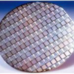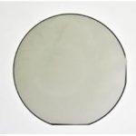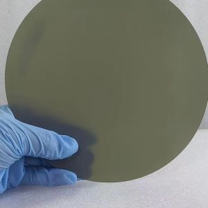

Freestanding GaN substrate
As a leading GaN substrate supplier, UNIELECTRON has established the manufacturing technology for freestanding (Gallium Nitride)GaN substrate wafer which is Bulk GaN substrate for UHB-LED, LD and fabrication as MOS-based devices. Grown by hydride vapour phase epitaxy (HVPE) technology, our GaN substrate for III-nitride devices has low defect density and less or free macro defect density. The GaN substrate thickness is 330~530μm.
In addition to power devices, gallium nitride semiconductor substrates are increasingly used in the manufacture of white light LEDs because the GaN LED substrates provide improved electrical characteristics and their performance exceeds current devices. Moreover, the rapid development of gallium nitride substrate technology has led to the development of high-efficiency GaN free standing substrates with low defect density and free macro defect density. Therefore, such GaN substrates can be increasingly used to white LEDs. As a result, the bulk GaN substrate market is growing rapidly. By the way, bulk GaN wafer can be used for testing vertical power device concepts.
1. Specification of Freestanding GaN substrate
Here shows detail specification:
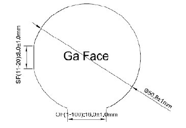
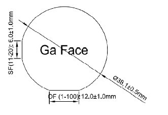
1.1 4″ N type Si doped GaN(Gallium Nitride) Free-standing Substrate
| Item | PAM-FS-GaN100-N+ |
| Conduction Type | N type/Si doped |
| Size | 4″(100)+/-1mm |
| Thickness | 480+/-50 |
| Orientation | C-axis(0001)+/-0.5o |
| Primary Flat Location | (10-10)+/-0.5o |
| Primary Flat Length | 32+/-1mm |
| Secondary Flat Location | (1-210)+/-3o |
| Secondary Flat Length | 18+/-1mm |
| Resistivity(300K) | <0.05Ω·cm |
| Dislocation Density | <5x106cm-2 |
| FWHM | <=100arc.sec |
| TTV | <=30um |
| BOW | <=+/-30um |
| Surface Finish | Front Surface:Ra<=0.3nm.Epi-ready polished |
| — | Back Surface:1.Fine ground |
| — | 2.Polished. |
| Usable Area | ≥ 90 % |
1.2 4″ N Type Low Doped GaN(Gallium Nitride) Free-standing Substrate
| Item | PAM-FS-GaN100-N- |
| Conduction Type | N type |
| Size | 4″(100)+/-1mm |
| Thickness | 480+/-50 |
| Orientation | C-axis(0001)+/-0.5o |
| Primary Flat Location | (10-10)+/-0.5o |
| Primary Flat Length | 32+/-1mm |
| Secondary Flat Location | (1-210)+/-3o |
| Secondary Flat Length | 18+/-1mm |
| Resistivity(300K) | <0.5Ω·cm |
| Dislocation Density | <5x106cm-2 |
| FWHM | <=100arc.sec |
| TTV | <=30um |
| BOW | <=+/-30um |
| Surface Finish | Front Surface:Ra<=0.3nm.Epi-ready polished |
| — | Back Surface:1.Fine ground |
| — | 2.Polished. |
| Usable Area | ≥ 90 % |
1.3 4″ Semi-Insulating GaN(Gallium Nitride) Free-standing Substrate
| Item | PAM-FS-GaN100-SI |
| Conduction Type | Semi-Insulating |
| Size | 4″(100)+/-1mm |
| Thickness | 480+/-50 |
| Orientation | C-axis(0001)+/-0.5o |
| Primary Flat Location | (10-10)+/-0.5o |
| Primary Flat Length | 32+/-1mm |
| Secondary Flat Location | (1-210)+/-3o |
| Secondary Flat Length | 18+/-1mm |
| Resistivity(300K) | >10^6Ω·cm |
| Dislocation Density | <5x106cm-2 |
| FWHM | <=100arc.sec |
| TTV | <=30um |
| BOW | <=+/-30um |
| Surface Finish | Front Surface:Ra<=0.3nm.Epi-ready polished |
| — | Back Surface:1.Fine ground |
| — | 2.Polished. |
| Usable Area | ≥ 90 % |
1.4 2″ Si doped GaN(Gallium Nitride) Free-standing Substrate
| Item | PAM-FS-GaN50-N+ | |||
| Conduction Type | N type/Si doped | |||
| Size | 2″(50.8)+/-1mm | |||
| Thickness | 400+/-50 | |||
| Orientation | C-axis(0001)+/-0.5o | |||
| Primary Flat Location | (10-10)+/-0.5o | |||
| Primary Flat Length | 16+/-1mm | |||
| Secondary Flat Location | (1-210)+/-3o | |||
| Secondary Flat Length | 8+/-1mm | |||
| Resistivity(300K) | <0.05Ω·cm | |||
| Dislocation Density | <5x106cm-2 | |||
| FWHM | <=100arc.sec | |||
| TTV | <=15um | |||
| BOW | <=+/-20um | |||
| Surface Finish | Front Surface:Ra<=0.3nm.Epi-ready polished | |||
| Back Surface:1.Fine ground | ||||
| 2.Polished. | ||||
| Usable Area | ≥ 90 % | |||
1.5 2″ Low doped GaN(Gallium Nitride) Free-standing Substrate
| Item | PAM-FS-GaN50-N- | ||||
| Conduction Type | N type | ||||
| Size | 2″(50.8)+/-1mm | ||||
| Thickness | 400+/-50 | ||||
| Orientation | C-axis(0001)+/-0.5o | ||||
| Primary Flat Location | (10-10)+/-0.5o | ||||
| Primary Flat Length | 16+/-1mm | ||||
| Secondary Flat Location | (1-210)+/-3o | ||||
| Secondary Flat Length | 8+/-1mm | ||||
| Resistivity(300K) | <0.5Ω·cm | ||||
| Dislocation Density | <5x106cm-2 | ||||
| FWHM | <=100arc.sec | ||||
| TTV | <=15um | ||||
| BOW | <=+/-20um | ||||
| Surface Finish | Front Surface:Ra<=0.3nm.Epi-ready polished | ||||
| Back Surface:1.Fine ground | |||||
| 2.Polished. | |||||
| Usable Area | ≥ 90 % | ||||
1.6 2″ Semi-Insulating GaN(Gallium Nitride) Free-standing Substrate
| Item | PAM-FS-GaN50-SI | ||||
| Conduction Type | Semi-Insulating | ||||
| Size | 2″(50.8)+/-1mm | ||||
| Thickness | 400+/-50 | ||||
| Orientation | C-axis(0001)+/-0.5o | ||||
| Primary Flat Location | (10-10)+/-0.5o | ||||
| Primary Flat Length | 16+/-1mm | ||||
| Secondary Flat Location | (1-210)+/-3o | ||||
| Secondary Flat Length | 8+/-1mm | ||||
| Resistivity(300K) | >10^6Ω·cm | ||||
| Dislocation Density | <5x106cm-2 | ||||
| FWHM | <=100arc.sec | ||||
| TTV | <=15um | ||||
| BOW | <=+/-20um | ||||
| Surface Finish | Front Surface:Ra<=0.3nm.Epi-ready polished | ||||
| Back Surface:1.Fine ground | |||||
| 2.Polished. | |||||
| Usable Area | ≥ 90 % | ||||
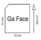
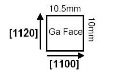
1.7 15mm,10mm,5mm Free-standing GaN Substrate
| Item | PAM-FS-GaN15-N | PAM-FS-GaN15-SI | |
| PAM-FS-GaN10-N | PAM-FS-GaN10-SI | ||
| PAM-FS-GaN5-N | PAM-FS-GaN5-SI | ||
| Conduction Type | N-type | Semi-insulating | |
| Size | 14.0mm*15mm 10.0mm*10.5mm 5.0*5.5mm | ||
| Thickness | 330-450um | ||
| Orientation | C-axis(0001)+/-0.5o | ||
| Primary Flat Location | |||
| Primary Flat Length | |||
| Secondary Flat Location | |||
| Secondary Flat Length | |||
| Resistivity(300K) | <0.5Ω·cm | >106Ω·cm | |
| Dislocation Density | <5x106cm-2 | ||
| Marco Defect Density | 0cm-2 | ||
| TTV | <=15um | ||
| BOW | <=20um | ||
| Surface Finish | Front Surface:Ra<0.2nm.Epi-ready polished | ||
| Back Surface:1.Fine ground | |||
| 2.Rough grinded | |||
| Usable Area | ≥ 90 % | ||
Note:
Validation Wafer: Considering convenience of usage, PAM-XIAMEN offers 2″ Sapphire Validation wafer for below 2″ size Freestanding GaN Substrate
2. Properties of Freestanding GaN Substrate
| Lattice Parameters | a=0.3189nm; c=0.5185nm |
| Band Gap | 3.39eV |
| Density | 6.15g/cm3 |
| Therm. Expansion Coefficient | a: 5.59×10⁻⁶/K; c: 3.17×10⁻⁶/K |
| Refraction Index | 2.33-2.7 |
| Dielectric Constant | 9.5 |
| Thermal Conductivity | 1.3W/(cm*k) |
| Break-Down Electrical Field | 3.3MV/cm |
| Saturation Drift Velocity | 2.5E7cm/s |
| Electron Mobility | 1300cm2/(V*s) |
3. Application of GaN Substrate
Solid State Lighting:GaN devices are used as ultra high brightness light emitting diodes (LEDs), TVs, automobiles, and general lighting
DVD Storage: Blue laser diodes
Power Device: Devices fabricated on GaN bulk substrate are used as various components in high-power and high-frequency power electronics like cellular base stations, satellites, power amplifiers, and inverters/converters for electric vehicles (EV) and hybrid electric vehicles (HEV). GaN’s low sensitivity to ionizing radiation (like other group III nitrides) makes it a suitable material for spaceborne applications such as solar cell arrays for satellites and high-power, high-frequency devices for communication, weather, and surveillance satellites
Pure Gallium Nitride Substrate Ideal for III-Nitrides re-growth
Wireless Base Stations: RF power transistors
Wireless Broadband Access: high frequency MMICs,RF-Circuits MMICs
Pressure Sensors:MEMS
Heat Sensors: Pyro-electric detectors
Power Conditioning: Mixed signal GaN/Si Integration
Automotive Electronics: High temperature electronics
Power Transmission Lines: High voltage electronics
Frame Sensors: UV detectors
Solar Cells: GaN’s wide band gap covers the solar spectrum from 0.65 eV to 3.4 eV (which is practically the entire solar spectrum), making indium gallium nitride
(InGaN) alloys perfect for creating solar cell material. Because of this advantage, InGaN solar cells grown on GaN substrates are poised to become one of the most important new applications and growth market for GaN substrate wafers.
Ideal for HEMTs, FETs
GaN Schottky diode project: We accept custom spec of Schottky diodes fabricated on the HVPE-grown, free-standing gallium nitride (GaN) layers of n- and p-types.
Both contacts (ohmic and Schottky) were deposited on the top surface using Al/Ti and Pd/Ti/Au.
Remark:
The Chinese government has announced new limits on the exportation of Gallium materials (such as GaAs, GaN, Ga2O3, GaP, InGaAs, and GaSb) and Germanium materials used to make semiconductor chips. Starting from August 1, 2023, exporting these materials is only allowed if we obtains a license from the Chinese Ministry of Commerce. Hope for your understanding and cooperation!
We will offer test reports, please see below an example:
Surface Roughness-GaN material-TEST REPORT
Transmitance-GaN material-TEST REPORT
XRD Rocking Curves-GaN Material-TEST REPORT
FREE STANDING GAN SINGLE CRYSTAL SUBSTRATES
10*10mm2 U-GaN Freestanding GaN Substrate
10*10mm2 Si-GaN Freestanding GaN Substrate
10*10mm2 N-GaN Freestanding GaN Substrate
A Plane U-GaN Freestanding GaN Substrate
A Plane N-GaN Freestanding GaN Substrate
A Plane Si-GaN Freestanding GaN Substrate
M Plane U-GaN Freestanding GaN Substrate
M Plane N-GaN Freestanding GaN Substrate
M Plane Si-GaN Freestanding GaN Substrate
(10-11) Plane U-GaN Freestanding GaN Substrate
(10-11) Plane N-GaN Freestanding GaN Substrate
(10-11) Plane Si-GaN Freestanding GaN Substrate
(11-22) Plane U-GaN Freestanding GaN Substrate
(11-22) Plane N-GaN Freestanding GaN Substrate
(11-22) Plane Si-GaN Freestanding GaN Substrate
(20-21) Plane U-GaN Freestanding GaN Substrate
(20-21) Plane N-GaN Freestanding GaN Substrate
(20-21) Plane Si-GaN Freestanding GaN Substrate
(20-2-1) Plane U-GaN Freestanding GaN Substrate
(20-2-1) Plane N-GaN Freestanding GaN Substrate
(20-2-1) Plane Si-GaN Freestanding GaN Substrate
Gallium Oxide(GaO) Wafer
100mm N Type GaN Substrate