
The LED epitaxial wafer is a substrate heated to an appropriate temperature. The LED wafer material is the cornerstone of the technology development for the semiconductor lighting industry. Different substrate materials require different LED epitaxial wafer growth technology, chip processing technology and device packaging technology. The substrate for LED epi wafer determines the development route of semiconductor lighting technology. To achieve luminous efficiency, epitaxial wafer suppliers pay more attention to GaN based LED epitaxial wafer, since the epitaxial wafer price is in low cost, and the epi wafer defect density is small. LED epi wafer advantage on GaN substrate is the realization of high efficiency, large area, single lamp and high power, which make the process technology simplify and improve the large yield rate. The development prospects of the LED epi wafer market are optimistic.
1. LED Wafer List
|
LED Epitaxial Wafer |
||||||||
| Item | Size | Orientation | Emission | Wavelength | Thickness | Substrate | Surface | Usable area |
| PAM-50-LED-BLUE-F | 50mm | 0°±0.5° | blue light | 445-475nm | 425um+/-25um | Sapphire | P/L | >90% |
| PAM-50-LED-BLUE-PSS | 50mm | 0°±0.5° | blue light | 445-475nm | 425um+/-25um | Sapphire | P/L | >90% |
| PAM-100-LED-BLUE-F | 100mm | 0°±0.5° | blue light | 445-475nm | / | Sapphire | P/L | >90% |
| PAM-100-LED-BLUE-PSS | 100mm | 0°±0.5° | blue light | 445-475nm | / | Sapphire | P/L | >90% |
| PAM-150-LED-BLUE | 150mm | 0°±0.5° | blue light | 445-475nm | / | Sapphire | P/L | >90% |
| PAM-100-LED-BLUE-SIL | 50mm | 0°±0.5° | blue light | 445-475nm | / | Silicon | P/L | >90% |
| PAM-100-LED-BLUE-SIL | 100mm | 0°±0.5° | blue light | 445-475nm | / | Silicon | P/L | >90% |
| PAM-150-LED-BLUE-SIL | 150mm | 0°±0.5° | blue light | 445-475nm | / | Silicon | P/L | >90% |
| PAM-200-LED-BLUE-SIL | 200mm | 0°±0.5° | blue light | 445-475nm | / | Silicon | P/L | >90% |
| PAM-50-LED-GREEN-F | 50mm | 0°±0.5° | green light | 510-530nm | 425um+/-25um | Sapphire | P/L | >90% |
| PAM-50-LED-GREEN-PSS | 50mm | 0°±0.5° | green light | 510-530nm | 425um+/-25um | Sapphire | P/L | >90% |
| PAM-100-LED-GREEN-F | 100mm | 0°±0.5° | green light | 510-530nm | / | Sapphire | P/L | >90% |
| PAM-100-LED-GREEN-PSS | 100mm | 0°±0.5° | green light | 510-530nm | / | Sapphire | P/L | >90% |
| PAM-150-LED-GREEN | 150mm | 0°±0.5° | green light | 510-530nm | / | Sapphire | P/L | >90% |
| PAM-100-LED-RED-GAAS-620 | 100mm | 15°±0.5° | red light | 610-630nm | / | GaAs | P/L | >90% |
| PAM210527-LED-660 | 100mm | 15°±0.5° | red light | 660nm | / | GaAs | P/L | >90% |
| PAM-210414-850nm-LED | 100mm | 15°±0.5° | IR | 850nm | / | GaAs | P/L | >90% |
| PAMP21138-940LED | 100mm | 15°±0.5° | IR | 940nm | / | GaAs | P/L | >90% |
| PAM-50-LED-UV-365-PSS | 50mm | 0°±0.5° | UVA | 365 nm | 425um+/-25um | Sapphire | ||
| PAM-50-LED-UV-405-PSS | 50mm | 0°±0.5° | UVA | 405 nm | 425um+/-25um | Sapphire | ||
| PAM-50-LED-UVC-275-PSS | 50mm | 0°±0.5° | UVC | 275nm | 425um+/-25um | Sapphire | ||
| PAM-50-LD-UV-405-SIL | 50mm | 0°±0.5° | UV | 405nm | / | Silicon | P/L | >90% |
| PAM-50-LD-BLUE-450-SIL | 50mm | 0°±0.5° | blue light | 450nm | / | Silicon | P/L | >90% |
As a LED epitaxial wafer manufacturer, PAM-XIAMEN can offer activated and unactivated GaN Epi LED wafer for LED and laser diodes (LD) application,such as For micro LED or ultra thin wafer or UV LED researches or LED manufacturers. LED epitaxial wafer on GaN is grown by MOCVD with PSS or flat sapphire for LCD back light, mobile, electronic or UV(ultraviolet), with blue or green or red emission, including InGaN/GaN active area and AlGaN layers with GaN well/AlGaN barrier for different chip sizes.
2. InGaN/GaN(gallium nitride) based LED Epitaxial Wafer
GaN on Al2O3-2” epi wafer Specification(LED Epitaxial wafer)
| White: 445~460 nm |
| Blue: 465~475 nm |
| Green: 510~530 nm |
1. Growth Technique – MOCVD
2.Wafer diameter: 50.8mm
3.Wafer substrate material: Patterned Sapphire Substrate(Al2O3) or Flat Sapphire
4.Wafer pattern size: 3X2X1.5μm
3. Wafer structure:
| Structure layers | Thickness(μm) |
| p-GaN | 0.2 |
| p-AlGaN | 0.03 |
| InGaN/GaN(active area) | 0.2 |
| n-GaN | 2.5 |
| u- GaN | 3.5 |
| Al2O3 (Substrate) | 430 |
4. Wafer parameters to make chips:
| em | Color | Chip Size | Characteristics | Appearance | |
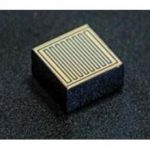
| PAM1023A01 | Blue | 10mil x 23mil |  |
Lighting | |
| Vf = 2.8~3.4V | LCD backlight | ||||
| Po = 18~25mW | Mobile appliances | ||||
| Wd = 450~460nm | Consumer electronic | ||||
| PAM454501 | Blue | 45mil x 45mil | Vf = 2.8~3.4V |  |
General lighting |
| Po = 250~300mW | LCD backlight | ||||
| Wd = 450~460nm | Outdoor display |
5. Application of LED epitaixal wafer:
*If you need to know more detail information of Blue LED Epitaxial Wafer, please contact with our sales departments
Lighting
LCD back light
Mobile appliances
Consumer electronic
6. Specification of LED Epi Wafer as an example:
Spec PAM190730-LED
– size : 4 inch
– WD : 455 ± 10nm
– brightness : > 90mcd
– VF : < 3.3V
– n-GaN Thickness : <4.1㎛
– u-GaN thickness : <2.2㎛
– substrate : patterned sapphire substrate (PSS)
7.GaAs(Gallium arsenide)based LED Wafer Material:
Regarding GaAs LED wafer, they are grown by MOCVD,see below wavelength of GaAs LED wafer:
Red:585nm,615nm,620~630nm
Yellow:587 ~ 592nm
Yellow/Green: 568 ~ 573nm
8. Definition of LED Epitaxial Wafer:
What we offer is bare LED epi wafer or not processed wafer without lithography processes, n- and metals contacts, etc. And you can fabricate the LED chip using your fabrication equipment for different application such as nano optoelectronics research.
Remark:
The Chinese government has announced new limits on the exportation of Gallium materials (such as GaAs, GaN, Ga2O3, GaP, InGaAs, and GaSb) and Germanium materials used to make semiconductor chips. Starting from August 1, 2023, exporting these materials is only allowed if we obtains a license from the Chinese Ministry of Commerce. Hope for your understanding and cooperation!
For these detail GaAs LED wafer specs,please visit:GaAs Epi Wafer for LED
For UV LED wafer specs,please visit:UV LED Epi Wafer
AlGaN UV LED Wafer
For LED wafer on silicon specs,please visit:LED Wafer on Silicon
For Blue GaN LD Wafer specs,please visit: Blue GaN LD Wafer
For Violet GaN LD Wafer, please visit: 405nm GaN Laser Diode Wafer
GaN LED Epi on Sapphire
850nm and 940nm infrared LED wafer
850-880nm and 890-910nm Red Infrared AlGaAs /GaAs LED Epi-Wafer
630nm GaAs LED Wafer
GaN Wafers to Fabricate LED Devices
GaN LED Structure Epitaxy on Flat or PSS Sapphire Substrate
GaN Epitaxial Growth on Sapphire for LED
Formation of V-Shaped Pits in Nitride Films Grown by Metalorganic Chemical Vapor Deposition
Si-based GaN PIN Photodetector Structure
For more foundry services, please visit: GaN Foundry Services for LED Fabrication