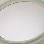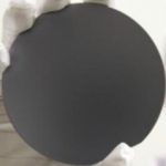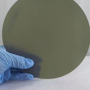

UNIELECTRON offers semiconductor SiC wafer Substrate, 6H SiC and 4H SiC (Silicon Carbide) in different quality grades for researcher and industry manufacturers. We has developed SiC crystal growth technology and SiC crystal wafer processing technology, established a production line to manufacture SiC substrate, Which is applied in GaN epitaxy device (e.g. AlN/GaN HEMT regrowth), power devices, high-temperature device and optoelectronic devices. As a professional silicon carbide wafer company invested by the leading manufacturers from the fields of advanced and high-tech material research and state institutes and China’s Semiconductor Lab, we are devoted to continuously improve the quality of currently SiC substrates and develop large size substrates.
Here shows detail specification:
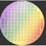
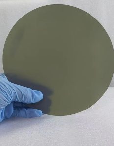
1. SiC Wafer Specifications
1.1 8″ SiC Wafer Specification
|
8 Inch N-type SiC Substrate |
|||
| Item | A Grade | B Grade | C Grade |
| Diameter | 200±0.2mm | ||
| Thickness | 500±25μm | ||
| Polytype | 4H | ||
| Surface Orientation | 4°toward <11-20>±0.5º | ||
| Dopant | n type Nitrogen | ||
| Notch Orientation | [1-100]±5° | ||
| Notch Depth | 1~1.5mm | ||
| Resistivity | 0.015~0.025 ohm·cm | 0.01~0.03 ohm·cm | NA |
| LTV | ≤5μm(10mm*10mm) | ≤10μm(10mm*10mm) | ≤15μm(10mm*10mm) |
| TTV | ≤10μm | ≤15μm | ≤20μm |
| BOW | -25μm~25μm | -45μm~45μm | -65μm~65μm |
| Warp | ≤35μm | ≤50μm | ≤70μm |
| Micropipe Density | ≤2ea/cm2 | ≤10ea/cm2 | ≤50ea/cm2 |
| Metal Content | ≤1E11 atoms/cm2 | ≤1E11 atoms/cm2 | NA |
| TSD | ≤500ea/cm2 | ≤1000ea/cm2 | NA |
| BPD | ≤2000ea/cm2 | ≤5000ea/cm2 | NA |
| TED | ≤7000ea/cm2 | ≤10000ea/cm2 | NA |
| Surface Roughness(Si-face) | Ra≤0.2nm | Ra≤0.2nm | Ra≤0.2nm |
| Front Surface Finished | Si-face CMP | ||
| Particle | ≤100(size≥0.3μm) | NA | NA |
| Scratches | ≤5,Total Length≤Diameter | NA | NA |
| Edge chips/indents/cracks/stains/ contamination |
None | None | NA |
| Polytype Areas | None | ≤20% (Cumulative area) | ≤30% (Cumulative area) |
| Front Marking | None | ||
| Back Surface Finished | C-face polished | ||
| Scratches | NA | NA | NA |
| Back defects edge chips/indents | None | None | NA |
| Back Roughness | Ra≤5nm | Ra≤5nm | Ra≤5nm |
| Back Marking | Notch(the right side) | ||
| Edge | Chamfer | Chamfer | Chamfer |
| Packaging | Epi-ready with vacuum packaging; Multi-wafer or Single wafer cassette packaging | ||
Notes: “NA”means no request. Items not mentioned may refer to SEMI-STD.
1.2 200mm Ultra-Prime SiC Substrate
| Item | 200mm N-Type SiC Wafer, DSP |
| Grade | Ultra Prime Grade |
| Diameter | 200±0.2mm |
| Thickness | 350±25um |
| Polytype | 4H |
| Dopant | N-type nitrogen |
| Orientation | 4° toward <11-20>±0.15° |
| Notch Orientation | {1-100}±5° |
| Notch depth | 1~1.5mm |
| Resitivity | 0.015~0.025Ω·cm |
| LTV | ≤3μm(10*10mm) |
| TTV | ≤7μm |
| Bow | -20~20um |
| Warp | ≤30μm |
| Si-face Roughness | Ra≤0.2nm |
| MPD | <0.2ea/cm2 |
| Metal impurities | ≤1E11 atoms/cm2(Al, Cr, Fe, Ni, Cu, Zn, Pb, Na, K, Ti, Ca, V, Mn) |
| TSD | ≤200ea/cm2 |
| BPD | ≤1000ea/cm2 |
| TED | ≤3000ea/cm2 |
| Front quality | |
| Front surface | Si |
| Surface finished | Si-face CMP |
| Particles | ≤100ea/wafer(Size≥0.3um) |
| Scratches | ≤5ea/nm, total length≤diameter |
| Edge Chips/indents/cracks/stains/contamination | None |
| Polytype areas | None |
| Front laser marking | None |
| Back quality | |
| Back finish | C-face polished |
| Scratches | NA |
| Back defects (edge chips/indents) | None |
| Back roughness | Ra≤5nm |
| Back laser marking | Notch to the right |
| Edge | Chamfer |
| Package | Epi-ready with vacuum packaging, multi-wafer/single wafer cassette |
1.3 150mm Ultra-Prime SiC Substrate
| Item | 150mm N-Type SiC Wafer, DSP |
| Grade | Ultra Prime Grade |
| Diameter | 150±0.2mm |
| Thickness | 350±25um |
| Polytype | 4H |
| Dopant | N-type nitrogen |
| Orientation | 4° toward <11-20>±0.15° |
| Primary Flat Orientation | {1-100}±5° |
| Primary Flat Length | 47.5±1.5mm |
| Secondary Flat | None |
| Resitivity | 0.016~0.024Ω·cm |
| LTV | ≤2μm(10*10mm) |
| TTV | ≤5μm |
| Bow | -15~15um |
| Warp | ≤20μm |
| Si-face Roughness | Ra≤0.2nm(5*5um) |
| MPD | <0.15ea/cm2 |
| Metal impurities | ≤5E10 atoms/cm2 |
| BPD | ≤600ea/cm2 |
| TSD | ≤100ea/cm2 |
| Front quality | |
| Front surface | Si |
| Surface finished | Si-face CMP |
| Particles | ≤60ea/wafer(Size≥0.3um) |
| Scratches | ≤2ea/nm, total length≤1/2*diameter |
| Orange peel/pits/cracks/contamination/stains/striations | None |
| Edge Chips/indents/fracture | None |
| Polytype areas | None |
| Front laser marking | None |
| Back quality | |
| Back finish | C-face polished |
| Scratches | ≤5ea/nm, total length≤diameter |
| Back defects (edge chips/indents) | None |
| Back roughness | Ra≤0.2nm(5*5um) |
| Back laser marking | 1mm from top edge |
| Edge | Chamfer |
| Package | Epi-ready with vacuum packaging, multi-wafer/single wafer cassette |
1.4 4H SIC,N-TYPE , 6″WAFER SPECIFICATION
| SUBSTRATE PROPERTY | S4H-150-N-PWAM-350 S4H-150-N-PWAM-500 | |
| Description | A/B Production Grade C/D Research Grade D Dummy Grade 4H SiC Substrate | |
| Polytype | 4H | 4H |
| Diameter | (150 ± 0.5) mm | (150 ± 0.5) mm |
| Thickness | (350 ± 25) μm (500 ± 25) μm | |
| Carrier Type | n-type | n-type |
| Dopant | n-type | n-type |
| Resistivity (RT) | (0.015 – 0.028)Ω·cm | (0.015 – 0.028)Ω·cm |
| Surface Roughness | < 0.5 nm (Si-face CMP Epi-ready); <1 nm (C- face Optical polish) | |
| FWHM | A<30 arcsec B/C/D <50 arcsec | |
| Micropipe Density | A≤0.5cm-2 B≤2cm-2 C≤15cm-2 D≤50cm-2 | |
| TTV | <15μm | <15μm |
| Bow | < 40μm | < 40μm |
| Warp | <60μm | <60μm |
| Surface Orientation | ||
| Off axis | 4° toward <11-20>± 0.5° | 4° toward <11-20>± 0.5° |
| Primary flat orientation | <11-20>±5.0° | <11-20>±5.0° |
| Primary flat length | 47.50 mm±2.00mm | 47.50 mm±2.00mm |
| Secondary flat | None | None |
| Surface Finish | Double face polished | Double face polished |
| Packaging | Single wafer box or multi wafer box | Single wafer box or multi wafer box |
| Cracks by high intensity list | None(A.B) | Cumulative length≤20mm,single length≤2mm (C.D) |
| Hex Plates by high intensity light | Cumulative area≤0.05%(A.B) | Cumulative area≤0.1%(C.D) |
| Polytype Areas by high intensity light | None(A.B) | Cumulative area≤3%(C.D) |
| Visual Carbon Inclusions | Cumulative area≤0.05%(A.B) | Cumulative area≤3%(C.D) |
| Scratches by high intensity light | None(A.B) | Cumulative length≤1 x wafer diameter (C.D) |
| Edge chip | None(A.B) | 5 allowed,≤1mm each (C.D) |
| Contamination by high intensity light | None | – |
| Usable area | ≥ 90 % | – |
| Edge exclusion | 3mm | 3mm |
1.5 4H SIC,HIGH PURITY SEMI-INSULATING(HPSI), 6″WAFER SPECIFICATION
4H SIC,V DOPED SEMI-INSULATING, 6″WAFER SPECIFICATION
| SUBSTRATE PROPERTY | S4H-150-SI-PWAM-500 | – |
| Description | A/B Production Grade C/D Research Grade D Dummy Grade 4H SiC Substrate | |
| Polytype | 4H | 4H |
| Diameter | (150 ± 0.5) mm | (150 ± 0.5) mm |
| Thickness | (500 ± 25) μm | (500 ± 25) μm |
| Carrier Type | Semi-insulating | Semi-insulating |
| Dopant | V doped | V doped |
| Resistivity (RT) | >1E7 Ω·cm | >1E7 Ω·cm |
| Surface Roughness | < 0.5 nm (Si-face CMP Epi-ready); <1 nm (C- face Optical polish) | |
| FWHM | A<30 arcsec B/C/D <50 arcsec | |
| Micropipe Density | A≤1cm-2 B≤5cm-2 C≤30cm-2 D≤50cm-2 | |
| TTV | <15μm | <15μm |
| Bow | < 40μm | < 40μm |
| Warp | <60μm | <60μm |
| Surface Orientation | ||
| On axis | <0001>± 0.5° | <0001>± 0.5° |
| Off axis | None | None |
| Primary flat orientation | <11-20>±5.0° | <11-20>±5.0° |
| Primary flat length | 47.50 mm±2.00mm | 47.50 mm±2.00mm |
| Secondary flat | None | None |
| Surface Finish | Double face polished | Double face polished |
| Packaging | Single wafer box or multi wafer box | Single wafer box or multi wafer box |
| Cracks by high intensity list | None(A.B) | Cumulative length≤20mm,single length≤2mm (C.D) |
| Hex Plates by high intensity light | Cumulative area≤0.05%(A.B) | Cumulative area≤0.1%(C.D) |
| Polytype Areas by high intensity light | None(A.B) | Cumulative area≤3%(C.D) |
| Visual Carbon Inclusions | Cumulative area≤0.05%(A.B) | Cumulative area≤3%(C.D) |
| Scratches by high intensity light | None(A.B) | Cumulative length≤1 x wafer diameter (C.D) |
| Edge chip | None(A.B) | 5 allowed,≤1mm each (C.D) |
| Contamination by high intensity light | None | – |
| Usable area | ≥ 90 % | – |
| Edge exclusion | 3mm | 3mm |
1.6 4H SIC,N-TYPE , 4″WAFER SPECIFICATION
| SUBSTRATE PROPERTY | S4H-100-N-PWAM-350 S4H-100-N-PWAM-500 | |
| Description | A/B Production Grade C/D Research Grade D Dummy Grade 4H SiC Substrate | |
| Polytype | 4H | 4H |
| Diameter | (100 ± 0.5) mm | (100 ± 0.5) mm |
| Thickness | (350 ± 25) μm (500 ± 25) μm | |
| Carrier Type | n-type | n-type |
| Dopant | Nitrogen | Nitrogen |
| Resistivity (RT) | (0.015 – 0.028)Ω·cm | (0.015 – 0.028)Ω·cm |
| Surface Roughness | < 0.5 nm (Si-face CMP Epi-ready); <1 nm (C- face Optical polish) | |
| FWHM | A<30 arcsec B/C/D <50 arcsec | |
| Micropipe Density | A≤0.5cm-2 B≤2cm-2 C≤15cm-2 D≤50cm-2 | |
| TTV | <10μm | <10μm |
| Bow | < 25μm | < 25μm |
| Warp | <45μm | <45μm |
| Surface Orientation | ||
| On axis | <0001>± 0.5° | <0001>± 0.5° |
| Off axis | 4°or 8° toward <11-20>± 0.5° | 4°or 8° toward <11-20>± 0.5° |
| Primary flat orientation | <11-20>±5.0° | <11-20>±5.0° |
| Primary flat length | 32.50 mm±2.00mm | 32.50 mm±2.00mm |
| Secondary flat orientation | Si-face:90° cw. from orientation flat ± 5°- | |
| C-face:90° ccw. from orientation flat ± 5°- | ||
| Secondary flat length | 18.00 ± 2.00 mm | 18.00 ± 2.00 mm |
| Surface Finish | Double face polished | Double face polished |
| Packaging | Single wafer box or multi wafer box | Single wafer box or multi wafer box |
| Cracks by high intensity list | None(A.B) | Cumulative length≤10mm,single length≤2mm (C.D) |
| Hex Plates by high intensity light | Cumulative area≤0.05%(A.B) | Cumulative area≤0.1%(C.D) |
| Polytype Areas by high intensity light | None(A.B) | Cumulative area≤3%(C.D) |
| Visual Carbon Inclusions | Cumulative area≤0.05%(A.B) | Cumulative area≤3%(C.D) |
| Scratches by high intensity light | None(A.B) | Cumulative length≤1 x wafer diameter (C.D) |
| Edge chip | None(A.B) | 5 allowed,≤1mm each (C.D) |
| Contamination by high intensity light | None | – |
| Usable area | ≥ 90 % | – |
| Edge exclusion | 2mm | 2mm |
1.7 4H SIC,HIGH PURITY SEMI-INSULATING(HPSI), 4″WAFER SPECIFICATION
4H SIC,V DOPED SEMI-INSULATING, 4″WAFER SPECIFICATION
| SUBSTRATE PROPERTY | S4H-100-SI-PWAM-350 S4H-100-SI-PWAM-500 | |
| Description | A/B Production Grade C/D Research Grade D Dummy Grade 4H SiC Substrate | |
| Polytype | 4H | 4H |
| Diameter | (100 ± 0.5) mm | (100 ± 0.5) mm |
| Thickness | (350 ± 25) μm (500 ± 25) μm | |
| Carrier Type | Semi-insulating | Semi-insulating |
| Dopant | V doped | V doped |
| Resistivity (RT) | >1E7 Ω·cm | >1E7 Ω·cm |
| Surface Roughness | < 0.5 nm (Si-face CMP Epi-ready); <1 nm (C- face Optical polish) | |
| FWHM | A<30 arcsec B/C/D <50 arcsec | |
| Micropipe Density | A≤1cm-2 B≤5cm-2 C≤30cm-2 D≤50cm-2 | |
| TTV | <10μm | <10μm |
| Bow | < 25μm | < 25μm |
| Warp | <45μm | <45μm |
| Surface Orientation | ||
| On axis | <0001>± 0.5° | <0001>± 0.5° |
| Off axis | None | None |
| Primary flat orientation | <11-20>±5.0° | <11-20>±5.0° |
| Primary flat length | 32.50 mm±2.00mm | 32.50 mm±2.00mm |
| Secondary flat orientation | Si-face:90° cw. from orientation flat ± 5°- | |
| C-face:90° ccw. from orientation flat ± 5°- | ||
| Secondary flat length | 18.00 ± 2.00 mm | 18.00 ± 2.00 mm |
| Surface Finish | Double face polished | Double face polished |
| Packaging | Single wafer box or multi wafer box | Single wafer box or multi wafer box |
| Cracks by high intensity list | None(A.B) | Cumulative length≤10mm,single length≤2mm (C.D) |
| Hex Plates by high intensity light | Cumulative area≤0.05%(A.B) | Cumulative area≤0.1%(C.D) |
| Polytype Areas by high intensity light | None(A.B) | Cumulative area≤3%(C.D) |
| Visual Carbon Inclusions | Cumulative area≤0.05%(A.B) | Cumulative area≤3%(C.D) |
| Scratches by high intensity light | None(A.B) | Cumulative length≤1 x wafer diameter (C.D) |
| Edge chip | None(A.B) | 5 allowed,≤1mm each (C.D) |
| Contamination by high intensity light | None | – |
| Usable area | ≥ 90 % | – |
| Edge exclusion | 2mm | 2mm |
1.8 4H N-TYPE SIC, 3″(76.2mm)WAFER SPECIFICATION
| SUBSTRATE PROPERTY | S4H-76-N-PWAM-330 S4H-76-N-PWAM-430 |
| Description | A/B Production Grade C/D Research Grade D Dummy Grade 4H SiC Substrate |
| Polytype | 4H |
| Diameter | (76.2 ± 0.38) mm |
| Thickness | (350 ± 25) μm (430 ± 25) μm |
| Carrier Type | n-type |
| Dopant | Nitrogen |
| Resistivity (RT) | 0.015 – 0.028Ω·cm |
| Surface Roughness | < 0.5 nm (Si-face CMP Epi-ready); <1 nm (C- face Optical polish) |
| FWHM | A<30 arcsec B/C/D <50 arcsec |
| Micropipe Density | A≤0.5cm-2 B≤2cm-2 C≤15cm-2 D≤50cm-2 |
| TTV/Bow /Warp | <25μm |
| Surface Orientation | |
| On axis | <0001>± 0.5° |
| Off axis | 4°or 8° toward <11-20>± 0.5° |
| Primary flat orientation | <11-20>±5.0° |
| Primary flat length | 22.22 mm±3.17mm |
| 0.875″±0.125″ | |
| Secondary flat orientation | Si-face:90° cw. from orientation flat ± 5° |
| C-face:90° ccw. from orientation flat ± 5° | |
| Secondary flat length | 11.00 ± 1.70 mm |
| Surface Finish | Single or double face polished |
| Packaging | Single wafer box or multi wafer box |
| Scratch | None |
| Usable area | ≥ 90 % |
| Edge exclusion | 2mm |
| Edge chips by diffuse lighting (max) | Please consult our engineer team |
| Cracks by high intensity light | Please consult our engineer team |
| Visual carbon Inclusions cumulative area | Please consult our engineer team |
| Scratches by high intensity light | Please consult our engineer team |
| Contamination by high intensity light | Please consult our engineer team |
1.9 4H SEMI-INSULATING SIC, 3″(76.2mm)WAFER SPECIFICATION
(High Purity Semi-Insulating(HPSI) SiC substrate is available)
| UBSTRATE PROPERTY | S4H-76-N-PWAM-330 S4H-76-N-PWAM-430 |
| Description | A/B Production Grade C/D Research Grade D Dummy Grade 4H SiC Substrate |
| Polytype | 4H |
| Diameter | (76.2 ± 0.38) mm |
| Thickness | (350 ± 25) μm (430 ± 25) μm |
| Carrier Type | semi-insulating |
| Dopant | V doped |
| Resistivity (RT) | >1E7 Ω·cm |
| Surface Roughness | < 0.5 nm (Si-face CMP Epi-ready); <1 nm (C- face Optical polish) |
| FWHM | A<30 arcsec B/C/D <50 arcsec |
| Micropipe Density | A≤1cm-2 B≤5cm-2 C≤30cm-2 D≤50cm-2 |
| TTV/Bow /Warp | <25μm |
| Surface Orientation | |
| On axis | <0001>± 0.5° |
| Off axis | 4°or 8° toward <11-20>± 0.5° |
| Primary flat orientation | <11-20>±5.0° |
| Primary flat length | 22.22 mm±3.17mm |
| 0.875″±0.125″ | |
| Secondary flat orientation | Si-face:90° cw. from orientation flat ± 5° |
| C-face:90° ccw. from orientation flat ± 5° | |
| Secondary flat length | 11.00 ± 1.70 mm |
| Surface Finish | Single or double face polished |
| Packaging | Single wafer box or multi wafer box |
| Scratch | None |
| Usable area | ≥ 90 % |
| Edge exclusion | 2mm |
| Edge chips by diffuse lighting (max) | Please consult our engineer team |
| Cracks by high intensity light | Please consult our engineer team |
| Visual carbon Inclusions cumulative area | Please consult our engineer team |
| Scratches by high intensity light | Please consult our engineer team |
| Contamination by high intensity light | Please consult our engineer team |
1.10 4H N-TYPE SIC, 2″(50.8mm)WAFER SPECIFICATION
| SUBSTRATE PROPERTY | S4H-51-N-PWAM-330 S4H-51-N-PWAM-430 |
| Description | A/B Production Grade C/D Research Grade D Dummy Grade 4H SiC Substrate |
| Polytype | 4H |
| Diameter | (50.8 ± 0.38) mm |
| Thickness | (250 ± 25) μm (330 ± 25) μm (430 ± 25) μm |
| Carrier Type | n-type |
| Dopant | Nitrogen |
| Resistivity (RT) | 0.012 – 0.0028 Ω·cm |
| Surface Roughness | < 0.5 nm (Si-face CMP Epi-ready); <1 nm (C- face Optical polish) |
| FWHM | A<30 arcsec B/C/D <50 arcsec |
| Micropipe Density | A≤0.5cm-2 B≤2cm-2 C≤15cm-2 D≤50cm-2 |
| Surface Orientation | |
| On axis | <0001>± 0.5° |
| Off axis | 4°or 8° toward <11-20>± 0.5° |
| Primary flat orientation | Parallel {1-100} ± 5° |
| Primary flat length | 16.00 ± 1.70) mm |
| Secondary flat orientation | Si-face:90° cw. from orientation flat ± 5° |
| C-face:90° ccw. from orientation flat ± 5° | |
| Secondary flat length | 8.00 ± 1.70 mm |
| Surface Finish | Single or double face polished |
| Packaging | Single wafer box or multi wafer box |
| Usable area | ≥ 90 % |
| Edge exclusion | 1 mm |
| Edge chips by diffuse lighting (max) | Please consult our engineer team |
| Cracks by high intensity light | Please consult our engineer team |
| Visual carbon Inclusions cumulative area | Please consult our engineer team |
| Scratches by high intensity light | Please consult our engineer team |
| Contamination by high intensity light | Please consult our engineer team |
1.11 4H SEMI-INSULATING SIC, 2″(50.8mm)WAFER SPECIFICATION
(High-Purity Semi-Insulating(HPSI) SiC substrate is available)
| SUBSTRATE PROPERTY | S4H-51-SI-PWAM-250 S4H-51-SI-PWAM-330 S4H-51-SI-PWAM-430 |
| Description | A/B Production Grade C/D Research Grade D Dummy Grade 4H SEMI Substrate |
| Polytype | 4H |
| Diameter | (50.8 ± 0.38) mm |
| Thickness | (250 ± 25) μm (330 ± 25) μm (430 ± 25) μm |
| Resistivity (RT) | >1E7 Ω·cm |
| Surface Roughness | < 0.5 nm (Si-face CMP Epi-ready); <1 nm (C- face Optical polish) |
| FWHM | A<30 arcsec B/C/D <50 arcsec |
| Micropipe Density | A≤1cm-2 B≤5cm-2 C≤30cm-2 D≤50cm-2 |
| Surface Orientation | |
| On axis <0001>± 0.5° | |
| Off axis 3.5° toward <11-20>± 0.5° | |
| Primary flat orientation | Parallel {1-100} ± 5° |
| Primary flat length | 16.00 ± 1.70 mm |
| Secondary flat orientation Si-face:90° cw. from orientation flat ± 5° | |
| C-face:90° ccw. from orientation flat ± 5° | |
| Secondary flat length | 8.00 ± 1.70 mm |
| Surface Finish | Single or double face polished |
| Packaging | Single wafer box or multi wafer box |
| Usable area | ≥ 90 % |
| Edge exclusion | 1 mm |
| Edge chips by diffuse lighting (max) | Please consult our engineer team |
| Cracks by high intensity light | Please consult our engineer team |
| Visual carbon Inclusions cumulative area | Please consult our engineer team |
| Scratches by high intensity light | Please consult our engineer team |
| Contamination by high intensity light | Please consult our engineer team |
1.12 6H N-TYPE SIC, 2″(50.8mm)WAFER SPECIFICATION
| SUBSTRATE PROPERTY | S6H-51-N-PWAM-250 S6H-51-N-PWAM-330 S6H-51-N-PWAM-430 |
| Description | A/B Production Grade C/D Research Grade D Dummy Grade 6H SiC Substrate |
| Polytype | 6H |
| Diameter | (50.8 ± 0.38) mm |
| Thickness | (250 ± 25) μm (330 ± 25) μm (430 ± 25) μm |
| Carrier Type | n-type |
| Dopant | Nitrogen |
| Resistivity (RT) | 0.02 ~ 0.1 Ω·cm |
| Surface Roughness | < 0.5 nm (Si-face CMP Epi-ready); <1 nm (C- face Optical polish) |
| FWHM | A<30 arcsec B/C/D <50 arcsec |
| Micropipe Density | A≤0.5cm-2 B≤2cm-2 C≤15cm-2 D≤50cm-2 |
| Surface Orientation | |
| On axis | <0001>± 0.5° |
| Off axis | 3.5° toward <11-20>± 0.5° |
| Primary flat orientation | Parallel {1-100} ± 5° |
| Primary flat length | 16.00 ± 1.70 mm |
| Secondary flat orientation | Si-face:90° cw. from orientation flat ± 5° |
| C-face:90° ccw. from orientation flat ± 5° | |
| Secondary flat length | 8.00 ± 1.70 mm |
| Surface Finish | Single or double face polished |
| Packaging | Single wafer box or multi wafer box |
| Usable area | ≥ 90 % |
| Edge exclusion | 1 mm |
| Edge chips by diffuse lighting (max) | Please consult our engineer team |
| Cracks by high intensity light | Please consult our engineer team |
| Visual carbon Inclusions cumulative area | Please consult our engineer team |
| Scratches by high intensity light | Please consult our engineer team |
| Contamination by high intensity light | Please consult our engineer team |
1.13 SiC Seed Crystal Wafer:
| Item | Size | Type | Orientation | Thickness | MPD | Polishing Condition |
| No.1 | 105mm | 4H, N type | C(0001)4deg.off | 500+/-50um | <=1/cm-2 | – |
| No.2 | 153mm | 4H, N type | C(0001)4deg.off | 350+/-50um | <=1/cm-2 | – |
4H N-type or semi-insulating SIC,5mm*5mm, 10mm*10mm WAFER SPECIFICATION: Thickness:330μm/430μm
4H N-type or semi-insulating SIC,15mm*15mm, 20mm*20mm WAFER SPECIFICATION:Thickness:330μm/430μm
a-plane SiC Wafer, size: 40mm*10mm,30mm*10mm,20mm*10mm,10mm*10mm,specs below:
6H/4H N type Thickness:330μm/430μm or custom
6H/4H Semi-insulating Thickness:330μm/430μm or custom
1.14 SILICON CARBIDE MATERIAL PROPERTIES
| SILICON CARBIDE MATERIAL PROPERTIES | ||
| Polytype | Single Crystal 4H | Single Crystal 6H |
| Lattice Parameters | a=3.076 Å | a=3.073 Å |
| c=10.053 Å | c=15.117 Å | |
| Stacking Sequence | ABCB | ABCACB |
| Band-gap | 3.26 eV | 3.03 eV |
| Density | 3.21 · 103 kg/m3 | 3.21 · 103 kg/m3 |
| Therm. Expansion Coefficient | 4-5×10⁻⁶/K | 4-5×10⁻⁶/K |
| Refraction Index | no = 2.719 | no = 2.707 |
| ne = 2.777 | ne = 2.755 | |
| Dielectric Constant | 9.6 | 9.66 |
| Thermal Conductivity | 490 W/mK | 490 W/mK |
| Break-Down Electrical Field | 2-4 · 108 V/m | 2-4 · 108 V/m |
| Saturation Drift Velocity | 2.0 · 105 m/s | 2.0 · 105 m/s |
| Electron Mobility | 800 cm2/V·S | 400 cm2/V·S |
| hole Mobility | 115 cm2/V·S | 90 cm2/V·S |
| Mohs Hardness | ~9 | ~9 |
2. About SiC Wafer
Silicon carbide wafer have excellent thermodynamic and electrochemical properties.
In terms of thermodynamics, the hardness of silicon carbide is as high as 9.2-9.3 on the Mohs at 20°C. It is one of the hardest materials and can be used to cut rubies. The SiC wafer thermal conductivity exceeds that of copper, which is 3 times that of Si and 8-10 times that of GaAs. And SiC wafer thermal stability is high, it is impossible to be melted under normal pressure.
In terms of electrochemistry, bare silicon carbide wafer has the characteristics of wide band gap and breakdown resistance. The band gap of SiC substrate wafer is 3 times that of Si, and breakdown electric field is 10 times that of Si, and its corrosion resistance is extremely strong.
Therefore, SiC-based SBDs and MOSFETs are more suitable for working in high-frequency, high-temperature, high-voltage, high-power, and radiation-resistant environments. Under the conditions of the same power level, SiC devices can be used to reduce the volume of electric drives and electronic controls, meeting the needs of higher power density and compact design. On the one hand, silicon carbide substrate wafer fabrication technology is mature, and the SiC wafer cost is competitive currently. On the other hand, the trend of intelligence and electrification continues to evolve. The traditional cars has brought huge demand for SiC power semiconductors. Thus, the global SiC wafer market is growing rapidly.
3. Q&A of SiC Wafer
3.1 What is the barrier of SiC wafer becoming a wide application same as silicon wafer?
1.Due to the physical and chemical stability of SiC, the crystal growth of SiC is extremely difficult, which seriously hinders the development of SiC semiconductor devices and their electronic applications.
2.Since there are many kinds of SiC structures with different stacking sequences (also known as polymorphism) , the growth of electronic grade SiC crystal is hindered. The polymorphs of SiC, such as 3C SiC, 4H SiC and 6h SiC.
3.2 What kind of SiC wafer do you offer?
What you need belongs to cubic phase, there are cubic (c), hexagonal (H) and rhombic (R). what we have are hexagonal, such as 4H and 6h, C is cubic, like 3C silicon carbide.
4. Please see below sub-catalogue:
4H N Type SiC
4H Semi-insulating SiC
SiC Ingots
Lapped Wafers
Polishing Wafer
100mm Silicon Carbide
200mm(8inch) SiC Wafers
6H SiC Wafer
PAM-XIAMEN Offers High Purity Semi-Insulating SiC substrate
SiC(Silicon Carbide) Boule Crystal
Sic Chips
HPSI SiC Wafer for Graphene Growth
Thick Silicon Carbide Substrate
Why do We Need High Purity Semi-insulating SiC Wafer?
Phonon Properties of SiC Wafer
Growth Facet
Why Does SiC Wafer Show Different Color?
4H-SiC Seed Crystal
P-Type SiC Substrate
3C SiC Wafer
200mm SiC Seed Wafer