
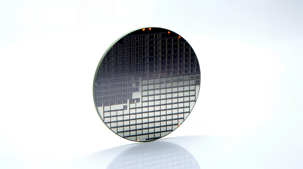
Gallium Nitride (GaN) wafers represent a significant advancement in semiconductor technology, particularly for applications requiring high power and high frequency. The unique properties of GaN make it an ideal choice for various industries, including telecommunications, automotive, and renewable energy. This article will explore the advantages of SAC GaN wafers and their transformative potential in the semiconductor market.
Key Advantages of GaN Wafers
- Wide Bandgap: GaN has a bandgap approximately three times wider than that of silicon. This characteristic allows GaN devices to operate at higher voltages, temperatures, and frequencies, making them suitable for high-performance applications.
- High Electron Mobility: The superior electron mobility in GaN enhances switching speeds and efficiency, enabling the development of faster and more efficient electronic devices. This property is crucial for applications such as RF amplifiers and power converters.
- High Thermal Conductivity: GaN wafers exhibit excellent thermal conductivity, which facilitates efficient heat dissipation. This capability is essential for maintaining device reliability in high-power applications, reducing the need for complex cooling systems.
- Compact Size and Lightweight: Due to their high power density, GaN devices can be smaller and lighter than their silicon counterparts. This miniaturization is particularly beneficial in portable electronics and automotive systems where space is at a premium.
- Chemical Stability: GaN’s resistance to oxidation and chemical degradation makes it suitable for harsh environments, ensuring longevity and reliability in demanding applications.
Applications of GaN Wafers GaN wafers are increasingly being utilized across various sectors due to their advantageous properties:
- Power Electronics: GaN is widely used in power amplifiers, DC-DC converters, and power supplies, particularly for electric vehicles and renewable energy systems like solar inverters.
- Telecommunications: The high-frequency capabilities of GaN make it ideal for RF devices used in wireless communications, satellite systems, and radar technologies.
- Optoelectronics: GaN plays a critical role in LED lighting and laser technologies due to its efficient light emission properties. This includes applications in displays, optical communications, and laser-based systems.
Market Trends The demand for GaN technology is on the rise. Companies like Infineon Technologies have recently developed 300 mm GaN wafer technology, significantly enhancing production efficiency by allowing more chips to be produced per wafer compared to traditional sizes. This advancement not only improves manufacturing scalability but also positions GaN wafers to achieve cost parity with silicon devices over time