
UNIELECTRON Advanced Material Co., Ltd (UNIELECTRON), a LD epitaxial wafer supplier, focuses on the GaAs and InP based laser diode epi wafers grown by MOCVD reactors for fiber-optic communication, industrial application, and special-purpose usage. UNIELECTRON can offer LD epitaxy wafer based on GaAs substrate for various fields, like VCSEL, infrared, photo-detector and etc. More details about the LD epitaxy wafer material, please refer to the table below:
| Substrate Material | Material Capability | Wavelength | Application |
| GaAs | GaAs/GalnP/AlGaInP/GaInP | 635nm | |
| GaAs Based Epi-wafer | 650nm | Vertical Cavity Surface Emitting Laser (VCSEL) RCLED |
|
| GaAs/GalnP/AlGaInP/GaInP | 660nm | ||
| GaAs/AlGaAs/GalnP/AlGaAs/GaAs | 703nm | ||
| GaAs/GalnP/AlGaInP/GaInP | 780nm | ||
| GaAs/GalnP/AlGaInP/GaInP | 785nm | ||
| GaAs Based Epi-wafer | 800-1064nm | Infrared LD | |
| GaAs/GalnP/AlGaInP/GaInP | 808nm | Infrared LD | |
| GaAs Based Epi-wafer | 850nm | Vertical Cavity Surface Emitting Laser (VCSEL) RCLED |
|
| GaAs Based Epi-wafer | <870nm | Photo-detector | |
| GaAs Based Epi-wafer | 850-1100nm | Vertical Cavity Surface Emitting Laser (VCSEL) RCLED |
|
| GaAs/AlGaAs/GaInAs/AlGaAs/GaAs | 905nm | ||
| GaAs/AlGaAs/InGaAs/AlGaAs/GaAs | 950nm | ||
| GaAs Based Epi-wafer | 980nm | Infrared LD | |
| InP Based Epi-wafer | 1250-1600nm | Avalanche photo-detector | |
| GaAs Based Epi-wafer | 1250-1600nm/>2.0um (InGaAs absorptive layer) |
Photo-detector | |
| GaAs Based Epi-wafer | 1250-1600nm/<1.4μm (InGaAsP absorptive layer) |
Photo-detector | |
| InP Based Epi-wafer | 1270-1630nm | DFB laser | |
| GaAsP/GaAs/GaAs substrate | 1300nm | ||
| InP Based Epi-wafer | 1310nm | FP laser | |
| GaAsP/GaAs/GaAs substrate | 1550nm | FP laser | |
| 1654nm | |||
| InP Based Epi-wafer | 1900nm | FP laser | |
| 2004nm |
About LD Epitaxy Wafer Applications & Market
The applications of GaAs based LD epitaxy wafer in the laser field can be divided into VCSELs and non-VCSELs. The current GaAs based LD epitaxy applications mainly lies in VCSELs. VCSEL (Vertical Cavity Surface Emitting Laser), based on GaAs materials, is mainly used for face recognition. It is expected to have a high growth rate in the future. EEL (Edge Emitting Laser) is a non-VCSEL device, mainly used in the field of automotive lidar, and the demand is expected to increase with the expansion of the driverless car market.
The GaAs substrate used in the laser field requires high technical indicators, and the unit epitaxial wafer price is significantly higher than that of other fields. The future LD epitaxial market space can be expected. Laser applications are the most sensitive to dislocation density. There is a high requirement for the GaAs substrate materials in laser applications. Therefore, the higher requirement is put forward on LD epitaxial wafer manufacturers and LD epitaxial wafer process. At present, the near-infrared band (760~1060 nm) semiconductor laser based on GaAs substrate has the most mature development and the most widespread application, and it has already been commercialized.
Remark:
The Chinese government has announced new limits on the exportation of Gallium materials (such as GaAs, GaN, Ga2O3, GaP, InGaAs, and GaSb) and Germanium materials used to make semiconductor chips. Starting from August 1, 2023, exporting these materials is only allowed if we obtains a license from the Chinese Ministry of Commerce. Hope for your understanding and cooperation!
Please see below detail specification of LD epitaxy wafer:
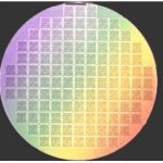
VCSEL Laser Wafer Chip
VCSEL Laser Epi Wafer
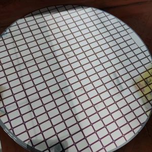
703nm laser diode epi wafer
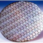
808nm laser diode epi wafer-1
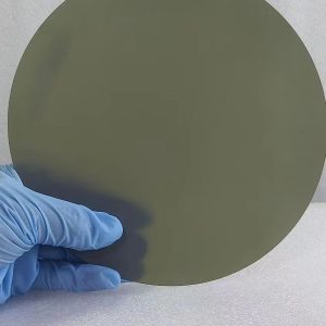
780nm laser diode epi wafer
650nm laser diode epi wafer
785nm laser diode epi wafer
808nm laser diode epi wafers-2
850nm laser diode epi wafer
905nm laser diode epi wafer
940nm laser diode epi wafer
950nm laser diode epi wafer
1060nm High Power Laser Wafer
1300nm Laser Diode Wafer
1460nm Pump Laser Diode Wafer
1550nm laser diode epi wafer
1654nm laser diode epi wafer
2004nm laser diode epi wafer
GaAs Epitaxy with Thick Growth
GaAs based Epi Structure MOCVD Grown for Light Emitter
Narrow InGaAsP Quantum Well Grown on InP Wafer
InAs Quantum Dot Layers on InP Substrate
FP (Fabry-Perot) Laser Wafer
PCSEL Wafer
Quantum Cascade Laser Wafer
Single Emitter Chips
Single-emitter LD Chip 755nm @8W
Single-emitter LD Chip 808nm @8W
Single-emitter LD Chip 808nm @10W
Single-emitter LD Chip 830nm @2W
Single-emitter LD Chip 880nm @8W
Single-emitter LD Chip 900+nm @10W
Single-emitter LD Chip 900+nm @15W
Single-emitter LD Chip 905nm @25W
Single-emitter LD Chip 1470nm @3W
PAM XIAMEN offers 1470 / 1550nm high power laser single chip as follows:
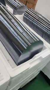
LD Bare Bar
LD Bare Bar for 780nm@cavity 2.5mm
LD Bare Bar for 808nm@cavity 2mm
LD Bare Bar for 808nm@cavity 1.5mm
LD Bare Bar for 880nm@cavity 2mm
LD Bare Bar for 940nm@cavity 2mm
LD Bare Bar for 940nm@cavity 3mm
LD Bare Bar for 940nm@cavity 4mm
LD Bare Bar for 940nm@cavity 2mm
LD Bare Bar for 976nm@cavity 4mm
LD Bare Bar for 1470nm@cavity 2mm
LD Bare Bar for 1550nm@cavity 2mm