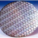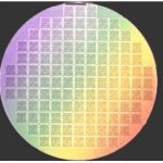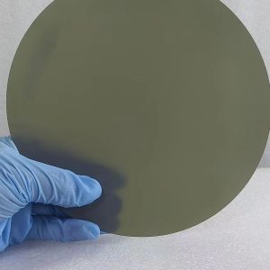

(Gallium Arsenide) GaAs Wafer
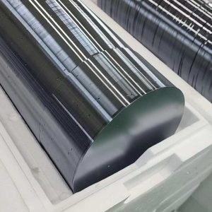
UNIELECTRON develops and manufactures compound semiconductor substrates-gallium arsenide crystal and wafer. We has used advanced crystal growth technology, vertical gradient freeze(VGF) and GaAs wafer manufacturing process, established a production line from crystal growth, cutting, grinding to polishing processing and built a 100-class clean room for GaAs wafer cleaning and packaging. Our GaAs wafers include 2~6 inch ingot/wafers for LED, LD and Microelectronics applications. We are always dedicated to improve the quality of currently GaAs wafer substrates and develop large size substrates. The GaAs wafer size offered is in 2”, 3”, 4” and 6”, and the thickness should be 220-700um. Moreover, the GaAs wafer price from us is competitive.
1. GaAs Wafer Specifications
1.1 (GaAs)Gallium Arsenide Wafers for LED Applications
| Item | Specifications | Remarks |
| Conduction Type | SC/n-type | SC/p-type with Zn dope Available |
| Growth Method | VGF | |
| Dopant | Silicon | Zn available |
| Wafer Diamter | 2, 3 & 4 inch | Ingot or as-cut availalbe |
| Crystal Orientation | (100)2°/6°/15° off (110) | Other misorientation available |
| OF | EJ or US | |
| Carrier Concentration | (0.4~2.5)E18/cm3 | |
| Resistivity at RT | (1.5~9)E-3 Ohm.cm | |
| Mobility | 1500~3000cm2/V.sec | |
| Etch Pit Density | <5000/cm2 | |
| Laser Marking | upon request | |
| Surface Finish | P/E or P/P | |
| Thickness | 220~450um | |
| Epitaxy Ready | Yes | |
| Package | Single wafer container or cassette | |
1.2 (GaAs)Gallium Arsenide Wafers for LD Applications
| Item | Specifications | Remarks |
| Conduction Type | SC/n-type | |
| Growth Method | VGF | |
| Dopant | Silicon | |
| Wafer Diamter | 2, 3 & 4 inch | Ingot or as-cut available |
| Crystal Orientation | (100)2°/6°/15°off (110) | Other misorientation available |
| OF | EJ or US | |
| Carrier Concentration | (0.4~2.5)E18/cm3 | |
| Resistivity at RT | (1.5~9)E-3 Ohm.cm | |
| Mobility | 1500~3000 cm2/V.sec | |
| Etch Pit Density | <500/cm2 | |
| Laser Marking | upon request | |
| Surface Finish | P/E or P/P | |
| Thickness | 220~350um | |
| Epitaxy Ready | Yes | |
| Package | Single wafer container or cassette | |
1.3 (GaAs)Gallium Arsenide Wafers,Semi-insulating for Microelectronics Applications
| Item | Specifications | Remarks |
| Conduction Type | Insulating | |
| Growth Method | VGF | |
| Dopant | C doped | |
| Wafer Diamter | 2, 3 & 4 inch | Ingot available |
| Crystal Orientation | (100)+/- 0.5° | |
| OF | EJ, US or notch | |
| Carrier Concentration | n/a | |
| Resistivity at RT | >1E7 Ohm.cm | |
| Mobility | >5000 cm2/V.sec | |
| Etch Pit Density | <8000 /cm2 | |
| Laser Marking | upon request | |
| Surface Finish | P/P | |
| Thickness | 350~675um | |
| Epitaxy Ready | Yes | |
| Package | Single wafer container or cassette | |
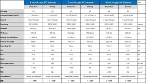
1.4 6″ (150mm)(GaAs)Gallium Arsenide Wafers,Semi-insulating for Microelectronics Applications
| Item | Specifications | Remarks |
| Conduction Type | Semi-insulating | – |
| Grow Method | VGF | – |
| Dopant | C doped | – |
| Type | N | – |
| Diamater(mm) | 150±0.25 | – |
| Orientation | (100)0°±3.0° | – |
| NOTCH Orientation | 〔010〕±2° | – |
| NOTCH Deepth(mm) | (1-1.25)mm 89°-95° | – |
| Carrier Concentration | please consult our sales team | – |
| Resistivity(ohm.cm) | >1.0×10⁷ | – |
| Mobility(cm2/v.s) | please consult our sales team | – |
| Dislocation | please consult our sales team | – |
| Thickness(µm) | 675±25 | – |
| Edge Exclusion for Bow and Warp(mm) | please consult our sales team | – |
| Bow(µm) | please consult our sales team | – |
| Warp(µm) | ≤20.0 | – |
| TTV(µm) | ≤10.0 | – |
| TIR(µm) | ≤10.0 | – |
| LFPD(µm) | please consult our sales team | – |
| Polishing | P/P Epi-Ready | – |
1.5 2″(50.8mm) LT-GaAs (Low Temperature-Grown Galium Arsenide) Wafer Specifications
| Item | Specifications |
| Conduction Type | Semi-insulating |
| Grow Method | VGF |
| Dopant | Sub:C doped / Epi:Undoped |
| Type | N |
| Diamater(mm) | 150±0.25 |
| Orientation | (100)0°±3.0° |
| NOTCH Orientation | 〔010〕±2° |
| NOTCH Deepth(mm) | (1-1.25)mm 89°-95° |
| Carrier Concentration | please consult our sales team |
| Resistivity(ohm.cm) | >1.0×10⁷ or 0.8-9 x10⁻³ |
| Mobility(cm2/v.s) | please consult our sales team |
| Dislocation | please consult our sales team |
| Thickness(µm) | 675±25 |
| Edge Exclusion for Bow and Warp(mm) | please consult our sales team |
| Bow(µm) | please consult our sales team |
| Warp(µm) | ≤20.0 |
| TTV(µm) | ≤10.0 |
| TIR(µm) | ≤10.0 |
| LFPD(µm) | please consult our sales team |
| Polishing | P/P Epi-Ready |
* We also can provide poly crystal GaAs bar, 99.9999%(6N).
* GaAs polycrystalline wafer with 7N purity is available, for specifications please refer to:
GaAs Polycrystalline Wafer
2. GaAs Wafer Market & Application
Gallium arsenide is an important semiconductor material. It belongs to group III-V compound semiconductors and the zinc blende crystal lattice structure, with a lattice constant of 5.65×10⁻¹⁰m, a melting point of 1237°C, and a band gap of 1.4 electron volts. Gallium arsenide can be made into semi-insulating high-resistance materials, which can be used to make integrated circuit substrates, infrared detectors, gamma photon detectors, etc. Because its electron mobility is 5 to 6 times greater than silicon, SI GaAs substrate has been importantly used in the fabrication of microwave devices and high-speed digital circuits. Semiconductor devices fabricated on gallium arsenide have the advantages of high frequency, high temperature, low temperature performance, low noise, and strong radiation resistance, which make the GaAs substrate market enlarge.
3. Test certificate of GaAs wafer can include below analysis if necessary:
1/Surface roughness of Gallium Arsenide including front side and backside(nanometers).
2/Doping concentration of Gallium Arsenide(cm-3)
3/EPD of Gallium Arsenide(cm-2)
4/Mobility of Gallium Arsendie(V.sec)
5/X-ray diffraction analysis (rocking curves) of Gallium Arsenide: Diffraction reflection curve half-width
6/Low-temperature photoluminescence (emission spectra in the range 0.7-1.0 μm) of Gallium Arsenide: The fraction of exciton photoluminescence in the emission spectrum of the near-IR range at a temperature of 4K or 5 K and an optical excitation density of 1 W / cm2
7/Transmission rate or Absorption coefficient: for instant, we can measure absorption coefficient of single crystal undoped GaAs at 1064nm: <0.6423 cm-1, and this corresponds to a transmission minimum of 33.2% for an exactly 6.5mm thick blank at 1064nm.
Remark:
The Chinese government has announced new limits on the exportation of Gallium materials (such as GaAs, GaN, Ga2O3, GaP, InGaAs, and GaSb) and Germanium materials used to make semiconductor chips. Starting from August 1, 2023, exporting these materials is only allowed if we obtains a license from the Chinese Ministry of Commerce. Hope for your understanding and cooperation!
Gallium Arsenide(GaAs) Wafer with High Mobility
Semi-insulating GaAs substrates 3 inch
Undoped Gallium Arsenide(GaAs) Wafer
Ultra Thin GaAs Wafer
Semi-insulating GaAs Substrate
P-type GaAs Substrates
N-type GaAs Wafer
GaAs Substrate for LED with Silicon Dopant
6 Inch Undoped GaAs Substrate, Prime & Mechanical Grade
GaAs Crystal with Low Defects and Dopants