
GaAs Epi wafer
As a leading GaAs epi wafer foundry, UNIELECTRON are manufacturing various types of epiwafer III-V silicon doped n-type semiconductor materials based on Ga, Al, In, As and P grown by MBE or MOCVD, which make a low gallium arsenide epi wafer defect. We supply custom GaAs epiwafer structures to meet customer specifications, please contact us for more information.
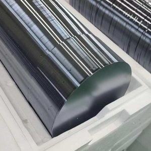
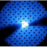
We have numbers of the United States Veeco’s GEN2000, GEN200 large-scale production of epitaxial equipment production line, full set of XRD; PL-Mapping; Surfacescan, and other world-class analysis and testing equipment. The company has more than 12,000 square meters of supporting plant, including world class super-clean semiconductor and a related research and development of the younger generation of clean laboratory facilities.
Specification for all new and featured products of MBE III-V compound semiconductor epitaxial wafer:
| Substrate Material | Material Capability | Application |
| GaAs | low temperature GaAs | THz |
| GaAs | GaAs/GaAlAs/GaAs/GaAs | Schottky Diode |
| InP | InGaAs | PIN detector |
| InP | InP/InP/InGaAsP/InP/InGaAs | Laser |
| GaAs | GaAs/AlAs/GaAs | |
| InP | InP/InAsP/InGaAs/InAsP | |
| GaAs | GaAs/InGaAsN/AlGaAs | |
| /GaAs/AlGaAs | ||
| InP | InP/InGaAs/InP | photodetectors |
| InP | InP/InGaAs/InP | |
| InP | InP/InGaAs | |
| GaAs | GaAs/InGaP/GaAs/AlInP | Solar Cell |
| /InGaP/AlInP/InGaP/AlInP | ||
| GaAs | GaAs/GaInP/GaInAs/GaAs/AlGaAs/GalnP/GalnAs | Solar Cell |
| /GalnP/GaAs/AlGaAs/AllnP/GalnP/AllnP/GalnAs | ||
| InP | InP/GaInP | |
| GaAs | GaAs/AlInP | |
| GaAs | GaAs/AlGaAs/GalnP/AlGaAs/GaAs | 703nm Laser |
| GaAs | GaAs/AlGaAs/GaAs | |
| GaAs | GaAs/AlGaAs/GaAs/AlGaAs/GaAs | HEMT |
| GaAs | GaAs/AlAs/GaAs/AlAs/GaAs | mHEMT |
| GaAs | GaAs/DBR/AlGaInP/MQW/AlGaInP/GaP | LED wafer,solid state lighting |
| GaAs | GaAs/GalnP/AlGaInP/GaInP | 635nm,660nm,808nm,780nm, 785nm, |
| /GaAsP/GaAs/GaAs substrate | 950nm, 1300nm,1550nm Laser | |
| GaSb | AlSb/GaInSb/InAs | IR detector,PIN,sensing, IR cemera |
| silicon | InP or GaAs on Silicon | High speed IC/microprocessors |
| InSb | Beryllium doped InSb | |
| / undoped InSb/Te doped InSb/ |
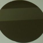
Gallium arsenide is currently one of the most important compound semiconductor materials with the highest mature epi wafer technology. GaAs material has the characteristics of large forbidden band width, high electron mobility, direct band gap, high luminous efficiency. Due to all all these epi wafer advantages, GaAs epitaxy is currently the most important material used in the field of optoelectronics. Meanwhile, it is also an important microelectronic material. According to the difference in electrical conductivity, GaAs epi wafer materials can be divided into semi-insulating (SI) GaAs and semiconductor (SC) GaAs.
In the field of epitaxial wafers, the epi wafer market share of RF and laser applications is very large.
For more detail specification, please review the following:
LT-GaAs epi layer on GaAs substrate
LT GaAs Thin Film for Photodetectors and Photomixers
Low Temperature Grown InGaAs
GaAs Schottky Diode Epitaxial Wafers
InGaAs/InP epi wafer for PIN
InGaAsP/InGaAs on InP substrates
InGaAs APD Wafers with High Performance
GaAs/AlAs wafer
InGaAsN epitaxially on GaAs or InP wafers
Structure for InGaAs photodetectors
InP/InGaAs/InP epi wafer
InGaAs Structure Wafer
AlGaP/GaAs Epi Wafer for Solar Cell
Triple-junction solar cells
Solar Cell Structure Epitaxially Grown on InP Wafer
GaAs Epitaxy
GaInP/InP epi wafer
AlInP/GaAs epi wafer
Growth of GaAsSb / InGaAs Type-II Superlattice
Layer structure of 703nm Laser
808nm laser wafers
780nm laser wafers
GaAs PIN epi wafer
AlGaAs / GaAs PIN Epitaxial Wafer
1550nm GaInAsP / InP PIN Photodiode Structure
InGaAs Photodiode Structure
GaAs/AlGaAs/GaAs epi wafer
GaAs HBT Epi Wafer
GaAs Based Epitaxial Wafer for LED and LD, please see below desc.
AlGaInP epi wafer
Yellow-Green AlGaInP/GaAs LED wafer:565-575nm
Positive LED Wafer Based on GaAs Substrate
Electroluminescence Testing of GaAs LED Epitaxial Wafer
GaAs HEMT epi wafer
GaAs pHEMT epi wafer (GaAs, AlGaAs, InGaAs), please see below desc.
GaAs mHEMT epi wafer (mHEMT: metamorphic high electron mobility transistor)
InP HEMT Epi Wafer
GaAs HBT epi wafer (GaAs HBT is bipolar junction transistors, which are composed of at least two different semiconductors,which is by GaAs based technology.)Metal-semiconductor field effect transistor (MESFET)
Heterojunction field effect transistor (HFET)
High electron mobility transistor (HEMT)
Pseudomorphic high electron mobility transistor (pHEMT)
Resonant tunnel diode (RTD)
PiN diode
hall effect devices
variable capacitance diode (VCD)
Performance of Terahertz Photoconductive Antennas
650 RC LED Wafer
650nm laser diode wafers
785nm laser diode wafers
808nm laser diode wafers
850nm laser diode wafers
905nm laser diode wafers
950nm laser diode wafers
1550nm laser diode wafers
1654nm laser diode wafers
2004nm laser diode wafers
PAM-XIAMEN Offers AlGaAs layer on GaAs substrate
GaAs substrate, 50 nm of InAlP, and then 2.5 microns of GaAs PAM210406-INALP
Now we list some specifications:
| GaAs HEMT epiwafer, size:2~6inch | ||
| Item | Specifications | Remark |
| Parameter | Al composition/In composition/Sheet resistance | Please contact our tech department |
| Hall mobility/2DEG Concentration | ||
| Measurement tech | X-ray diffraction/Eddy current | Please contact our tech department |
| Un-contact hall | ||
| Typical valve | Struture dependent | Please contact our tech department |
| 5000~6500cm2/V ·S/0.5~1.0x 1012cm-2 | ||
| Standard tolerance | ±0.01/±3%/none | Please contact our tech department |
| GaAs(gallium arsenide) pHEMT epiwafer, size:2~6inch | ||
| Item | Specifications | Remark |
| Parameter | Al composition/In composition/Sheet resistance | Please contact our tech department |
| Hall mobility/2DEG Concentration | ||
| Measurement tech | X-ray diffraction/Eddy current | Please contact our tech department |
| Un-contact hall | ||
| Typical valve | Struture dependent | Please contact our tech department |
| 5000~6800cm2/V ·S/2.0~3.4x 1012cm-2 | ||
| Standard tolerance | ±0.01/±3%/none | Please contact our tech department |
| Remark:GaAs pHEMT: Compared with GaAs HEMT, GaAs PHEMT also incorporates InxGa1-xAs,where InxAs is constrained to x < 0.3 for GaAs-based devices. Structures grown with the same lattice constant as HEMT, but different band gaps are simply referred to as lattice-matched HEMTs. | ||
| GaAs mHEMT epiwafer, size:2~6inch | ||
| Item | Specifications | Remark |
| Parameter | In composition/Sheet resistance | Please contact our tech department |
| Hall mobility/2DEG Concentration | ||
| Measurement tech | X-ray diffraction/Eddy current | Please contact our tech department |
| Un-contact hall | ||
| Typical valve | Struture dependent | Please contact our tech department |
| 8000~10000cm2/V ·S/2.0~3.6x 1012cm-2 | ||
| Standard tolerance | ±3%/none | Please contact our tech department |
| InP HEMT epiwafer, size:2~4inch | ||
| Item | Specifications | Remark |
| Parameter | In composition/Sheet resistance/Hall mobility | Please contact our tech department |
Remark: GaAs(Gallium arsenide) is a compound semiconductor material,a mixture of two elements, gallium (Ga) and arsenic (As). The uses of Gallium arsenide are varied and include being used in LED/LD, field-effect transistors (FETs), and integrated circuits (ICs)
Device applications
RF Switch, Power and low-noise amplifiers, Hall sensor, Optical modulator
Wireless: cell phone or base stations
Automotive radar, MMIC, RFIC, Optical Fiber Communications
GaAs Epi Wafer for LED/IR serie:
1.General description:
1.1 Growth Method: MOCVD
1.2 GaAs epi wafer for Wireless Networking
1.3 GaAs epi wafer for LED /IR and LD/PD
2.Epi wafer specs:
2.1 Wafer size: 2”diameter
2.2 GaAs Epi Wafer Structure(from top to bottom):
P + GaAs
p-GaP
p-AlGaInP
MQW-AlGaInP
n-AlGaInP
DBR n-ALGaAs / AlAs
Buffer
GaAs substrate
3.Chip sepcification (Base on 9mil*9mil chips)
3.1 Parameter
Chip Size 9mil*9mil
Thickness 190±10um
Electrode diameter 90um±5um
3.2 Optical-elctric characters(Ir=20mA,22℃)
Wavelength 620~625nm
Forward voltage 1.9~2.2v
Reverse voltage ≥10v
Reverse current 0-1uA
3.3 Light intensity characters(Ir=20mA,22℃)
IV (MCD) 80-140
3.4 Epiwafer avelength
|
Item |
Unit |
Red |
Yellow |
Yellow/Green |
Description |
|
Wave Length (λD) |
nm |
585,615,620 ~ 630 |
587 ~ 592 |
568 ~ 573 |
IF =20mA |
Growth Methods:MOCVD,MBE
epitaxy = growth of film with a crystallographic relationship between film and substrate homoepitaxy (autoepitaxy, isoepitaxy) = film and substrate are same material heteroepitaxy = film and substrate are different materials. For more information of growth methods, please click the following: https://www.powerwaywafer.com/technology.html
Remark:
The Chinese government has announced new limits on the exportation of Gallium materials (such as GaAs, GaN, Ga2O3, GaP, InGaAs, and GaSb) and Germanium materials used to make semiconductor chips. Starting from August 1, 2023, exporting these materials is only allowed if we obtains a license from the Chinese Ministry of Commerce. Hope for your understanding and cooperation!
InGaAs Epitaxy Sensor / Detector:
Shortwave Infrared InGaAs Sensor
InGaAs SWIR Detector
InGaAs/InAlAs Epistucture for Single Photon Detector
Epiwafer for Photonic Integrated Chip:
AlGaAs Thin Film Epitaxy for Photonic Integrated Chips