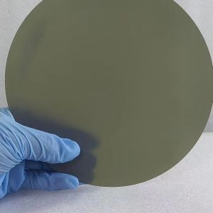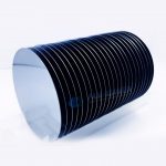

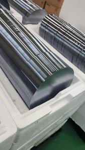
InP wafer
UNIELECTRON, a leading InP wafer supplier, offers Compound Semiconductor InP wafer – Indium Phosphide which are grown by LEC(Liquid Encapsulated Czochralski) or VGF(Vertical Gradient Freeze) as epi-ready or mechanical grade with n type, p type or semi-insulating. The InP wafer orientation (111) or (100) is available. And the dopants can be Sulphur, Sn(Tin), Zinc or customs. The Laser Mark as specified on backside of InP wafer along with primary flat. The orientation with slight deflection angle is available, such as (100)0.075° towards [110]]±0.025°.
Indium phosphide (InP) is a binary semiconductor composed of indium and phosphorus. It has a face-centered cubic (“zinc blende”) crystal structure, identical to that of GaAs and most of the III-V semiconductors. Indium phosphide can be prepared from the reaction of white phosphorus and indium iodide [clarification needed] at 400 °C., also by direct combination of the purified elements at high temperature and pressure, or by thermal decomposition of a mixture of a trialkyl indium compound and phosphide. Indium phosphide wafers are used in high-power and high-frequency electronics [citation needed] because of the superior electron velocity with respect to the more common semiconductors silicon and gallium arsenide. The InP wafer size we can offer is 2”, 3” and 4”, and the InP wafer thickness will be 350~625um.
Here is the detail specification:
2″ InP Wafer Specification
| Item | Specifications | |||
| Dopant | N-type | N-type | P-type | SI-type |
| Conduction Type | low doped | Sulphur | Zinc | lron |
| Wafer Diameter | 2″ | |||
| Wafer Orientation | (100)±0.5° | |||
| Wafer Thickness | Min:325 Max:375 | |||
| Primary Flat Length | 16±2mm | |||
| Secondary Flat Length | 8±1mm | |||
| Carrier Concentration | 3×1016cm-3 | (0.8-6)x1018cm-3 | (0.6-6)x1018cm-3 | N/A |
| Mobility | (3.5-4)x103cm2/V.s | (1.5-3.5)x103cm2/V.s | 50-70×103cm2/V.s | >1000cm2/V.s |
| Resistivity | N/A | N/A | N/A | N/A |
| EPD | <1000cm-2 | <500cm-2 | <1×103cm-2 | <5×103cm-2 |
| TTV | <10um | |||
| BOW | <10um | |||
| WARP | <12um | |||
| Laser marking | upon request | |||
| Suface finish | P/E, P/P | |||
| Epi ready | yes | |||
| Package | Single wafer container or cassette | |||
2″ P Type InP Wafer Specification
| Item | Parameter | UOM |
| Material | InP | |
| Conduct Type/Dopant | S-C-P/Zn | |
| Grade | Prime | |
| Diameter: | 50.5±0.4 | mm |
| Orientation: | (100)±0.5° | |
| Orientation Angle: | / | |
| Thickness: | Min:325 Max:375 | um |
| Carrier Concentration: | Min:0.6E18 Max:3E18 | cm-3 |
| Resistivity: | Min:/ Max:/ | ohm.cm |
| Mobility: | Min:/ Max:/ | cm-2/V.sec |
| EPD: | Ave<:1000 Max<:/ | cm-2 |
| TTV: | Max:10 | um |
| TIR: | Max:10 | um |
| BOW: | Max:10 | um |
| Warp: | Max:15 | um |
| Flat Option: | EJ | |
| Primary Flat Orientation: | (0-1-1) | |
| Primary Flat Length: | 16±1 | mm |
| Secondary Flat Orientation: | (0-11) | |
| Secondary Flat Length: | 7±1 | mm |
| Suface: | Side 1:Polished Side 2:etched | |
| Edge Rounding | 0.25(Conform to SEMI Standards) | mmR |
| Particle Count: | / | |
| Package | individual container filled with N2 | |
| Epi-ready | Yes | |
| Laser Marking | Back side major flat | |
| Remark: | Special specifications will be discussed separately | |
3″ InP Wafer Specification
| Item | Specifications | |||
| Dopant | N-type | N-type | P-type | SI-type |
| Conduction Type | low doped | Sulphur | Zinc | lron |
| Wafer Diameter | 3″ | |||
| Wafer Orientation | (100)±0.5° | |||
| Wafer Thickness | 600±25um | |||
| Primary Flat Length | 16±2mm | |||
| Secondary Flat Length | 8±1mm | |||
| Carrier Concentration | ≤3×1016cm-3 | (0.8-6)x1018cm-3 | (0.6-6)x1018cm-3 | N/A |
| Mobility | (3.5-4)x103cm2/V.s | (1.5-3.5)x103cm2/V.s | 50-70×103cm2/V.s | >1000cm2/V.s |
| Resistivity | N/A | N/A | N/A | N/A |
| EPD | <1000cm-2 | <500cm-2 | <1×103cm-2 | <5×103cm-2 |
| TTV | <12um | |||
| BOW | <12um | |||
| WARP | <15um | |||
| Laser marking | upon request | |||
| Suface finish | P/E, P/P | |||
| Epi ready | yes | |||
| Package | Single wafer container or cassette | |||
4″ InP Wafer Specification
| Item | Specifications | |||
| Dopant | N-type | N-type | P-type | SI-type |
| Conduction Type | low doped | Sulphur | Zinc | lron |
| Wafer Diameter | 4″ | |||
| Wafer Orientation | (100)±0.5° | |||
| Wafer Thickness | 600±25um | |||
| Primary Flat Length | 16±2mm | |||
| Secondary Flat Length | 8±1mm | |||
| Carrier Concentration | ≤3×1016cm-3 | (0.8-6)x1018cm-3 | (0.6-6)x1018cm-3 | N/A |
| Mobility | (3.5-4)x103cm2/V.s | (1.5-3.5)x103cm2/V.s | 50-70×103cm2/V.s | >1000cm2/V.s |
| Resistivity | N/A | N/A | N/A | N/A |
| EPD | <1000cm-2 | <500cm-2 | <1×103cm-2 | <5×103cm-2 |
| TTV | <15um | |||
| BOW | <15um | |||
| WARP | <15um | |||
| Laser marking | upon request | |||
| Suface finish | P/E, P/P | |||
| Epi ready | yes | |||
| Package | Single wafer container or cassette | |||
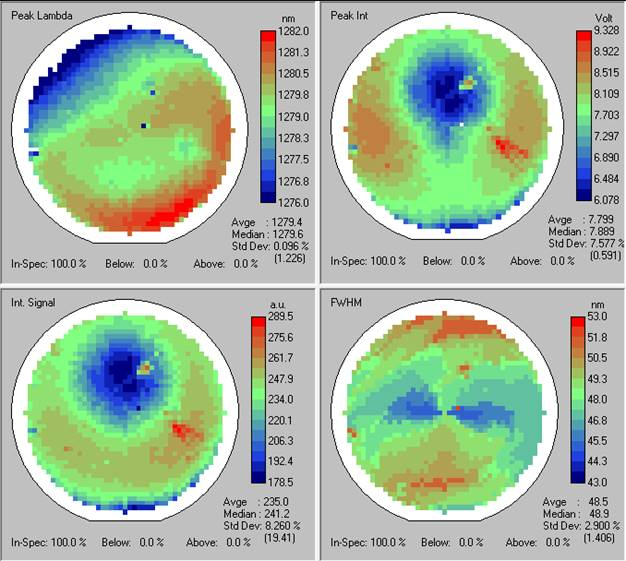
PL(Photoluminescence) Test of Indium Phosphide Wafer
We measure InP wafers by Peak Lambda, Peak int, and FWHM, the spectra mapping is as follows:
About InP Wafer Application
As a new type of compound semiconductor material, InP wafer market share is increasing gradually. Due to the excellent indium phosphide properties, the performance of microwave power source devices, microwave amplifiers and gate FETs fabricated on InP material will be better than those fabricated on existing gallium arsenide materials. Indium phosphide heterojunction lasers are also extremely promising light sources in optical fiber communications.
InP wafer fabrication for devices, like growing millimeter wave microelectronic devices and optoelectronic device materials for optical fiber communications, is widely used. With the continuous improvement of device performance and the reduction of device size, the quality requirements for indium phosphide wafers are getting higher and higher. Therefore, the InP wafer process is optimizing gradually.
The the typical values is see below data:
| Peak Lambda(nm) | Peak Int | FWHM(nm) |
| 1279.4 | 7.799 | 48.5 |
| 1279.8 | 5.236 | 44.6 |
Undoped InP Wafer
Prime Grade Semi-insulating Indium Phosphide
Dummy Grade Indium Phosphide Wafer
InAs Quantum Dot Layers on InP Substrate
Safety Data Sheet of Indium Phosphide Wafer
P Type Indium Phosphide Semiconductor Substrate