
Grade
Production Grade
(P Grade)
Research Grade
(R Grade)
Dummy Grade(D Grade)
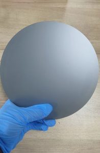
Diameter 50.8mm±0.38mm
Thickness 350μm ± 25μm
Wafer Orientation Off axis: 2.0°-4.0°toward [1120]±0.5°for 4H/6H-P, On axis: (111)±0.5°for 3C-N
Micropipe Density 0cm-2
Resistivity 4H/6H-P ≤ 0.1ω.cm
3C-N ≤ 0.8mω.cm
Primary Flat Orientation 4H/6H-P. Primary flat orientation 4h / 6h-p
3C-N {10-10}±5.0°
1-10} {+ / – 5.0 °
The Primary Flat Length is 15.9 mm±1.7 mm
Secondary Flat Length 8.0 mm±1.7mm
Secondary Flat Orientation Silicon face up: 90°CW. from Prime flat ±5.0°
Edge Exclusion 3 mm 3mm
TTV Warp ≤ 2.5μm /≤ 5μm /≤15
μm/≤30 μm
Roughness Polish Ras1 nm
CMP Ras0.2nm
Edge Cracks By High Intensity Light None 1 allowed, s1 mm
Hex Plates By High Intensity Light Cumulative areas1 % Cumulative areas3 %
Polytype Areas By High Intensity Light None Cumulative areas2% Cumulative areas5%
Si
Silicon Surface Scratches By High Intensity Light 3 scratches to 1xwafer diameter cumulative length 5 scratches to 1xwafer diameter cumulative length 8 scratches to 1xwafer diameter
cumulative length
Edge Chips High By Intensity Light light None 3 allowed, ≤ 0.5mm each 5 allowed, ≤1 mm each
Silicon Surface Contamination By High Intensity None
Packaging Multi-wafer Cassette or Single Wafer Container