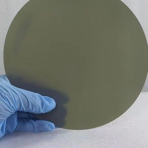

UNIELECTRON offers 300mm silicon oxide wafer and dioxide wafer. Thermal oxide silicon wafer or silicon dioxide wafer is a bare silicon wafer with oxide layer grown by dry or wet oxidation process. The thermal oxide layer of the silicon wafer is usually grown in a horizontal tube furnace, and the silicon wafer oxide temperature range is generally 900 ℃ ~ 1200 ℃. Compared with CVD oxide layer, silicon wafer oxide layer has higher uniformity, better compactness, higher dielectric strength and better quality.
1. Parameters of Silicon Oxide Wafer
| Parameters | Value |
| Type of ingot | Grown according to the Czochralski method |
| Diametr, mm | 300 ± 0,2 |
| Wafers Life time, month | 12 |
| Conductivity type | P |
| Dopant | B (boron) |
| Oxigen max, OLD-PPMA | 40 |
| Carbon , PPMA | 1 |
| The exclusion of the edge zone, mm | 3 |
| Crystallographic orientation | <100> |
| Deviation of surface orientation from a given crystallographic plane, degrees | 0,5 |
| Volume resistivity, Ohm · cm | 10-40 |
| The number of dislocations, cm-2 | 0 |
| The number of point etching defects, cm-2 | 0 |
| The number of point oxidative defects, cm -2 | 500 |
| The maximum iron content in the volume, E10AT/CC | 10 |
| Primary Notch | yes |
| Notch Location | 110 |
| Notch size, mm | 2,3 |
| Notch Form | V |
| Wafer thickness, microns | 775±25 |
| Type of marking | Laser |
| Marking Location | back side |
| Edge profile | By SEMI T / 4 |
| Front scratches | absent |
| Total wafer thickness change (TTV), microns | 5 |
| Deflection, microns | 60 |
| Wafers are oxidized to a thickness, microns | 0,1-1 |
| The number of particles on a surface larger than 0.09 microns | 50 |
| Contamination of the back side | absent |
| Surface content of aluminium, E10AT/CM2 | 1 |
| Surface content of calcium, E10AT/CM2 | 1 |
| Surface content of chromium, E10AT/CM2 | 1 |
| Surface content of copper, E10AT/CM2 | 1 |
| Surface content of iron, E10AT/CM2 | 1 |
| Surface content of potassium, E10AT/CM2 | 1 |
| Surface content of natrium, E10AT/CM2 | 1 |
| Surface content of nickel, E10AT/CM2 | 1 |
| Surface content of zinc, E10AT/CM2 | 1 |
| Requirements for the accuracy of flatness, microns | 0,3 |
| The exclusion of the edge zone when measuring flatness, mm | 3 |
Packing requirements:
| Parameter | |
| Type of packaging | MW300GT-A |
| Inner Container Material | Polyethylene |
| Outer Packing Material | Aluminum |
| Number of pieces in one package | 25 |
| Reusability | yes |
2. Oxidation Methods
Dry oxidation and wet oxidation are the most important methods for growing silicon on oxide wafer.
2.1 Dry oxidation silicon wafer
Dry oxygen oxidation silicon reacts with oxygen at the temperature of 850-1200 ℃, the rate of thermal oxide growth silicon wafers is low but the quality is good, so it can be used for MOS insulated gate growth. Silicon wafer oxide thickness is 10nm~300nm.
2.2 Wet oxygen oxidation wafer
At high temperature, water vapor is used to enter the furnace tube and form oxide layer on the surface of silicon wafer. The density of wet oxygen oxidation is slightly worse than that of dry oxygen oxidation, but the advantage of wet oxygen oxidation is that it has a higher growth rate, which is suitable for the film growth above 500 nm. Wet oxidation capacity: 100nm~6um.
During the silicon wafer oxidation process, the thermal silicon oxide wafer is an excellent dielectric layer as an insulator. In many silicon-based devices, the thermal oxide layer plays an important role as a doping prevention layer and a surface dielectric.
3. FAQ:
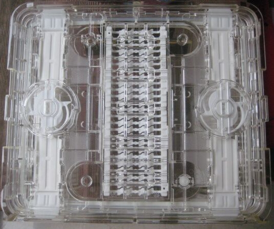
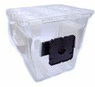
Could you please check if accept the packaging MW300GT-A as attached picture?
— Yes, please go ahead.
send us email at [email protected] and [email protected]
2″ Monocrystalline silicon wafers with insulating oxide
2″ Monocrystalline Silicon Wafer with Thermal Oxide 20nm
4″ Monocrystalline silicon wafers with insulating oxide
4″ Monocrystalline Silicon Wafer with Thermal oxide 20nm
6″ Monocrystalline silicon wafers with insulating oxide
6″ Monocrystalline Silicon Wafer with Thermal Oxide 20nm
2″ Silicon Oxide Wafer
3″ Silicon Oxide Wafer
4″ Silicon Oxide Wafer