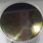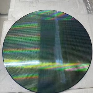

UNIELECTRONoffers 300mm P type or N type test silicon wafer (12 inch). The silicon test wafer thickness is 775±25μm. Compared to other silicon wafer suppliers, Powerway Wafer offers professional service with competitive prices.
1. Specification of Test Silicon Wafer
| Parameters | Value |
| Type of ingot | Grown according to the Czochralski method |
| Diameter, mm | 300 ± 0,2 |
| Dopant | B (boron) |
| Conductivity type | P |
| Oxigen max, OLD-PPMA | 40 |
| Carbon , PPMA | 1 |
| Test silicon wafer crystal orientation | <100> |
| Deviation from the predetermined surface orientation of crystal plane, deg | 1 |
| Volume resistivity, Ohm · cm | 10-40 |
| Primary Notch | Yes |
| Notch Location | 110 |
| Notch size, mm | 2,3 |
| Notch Form | V |
| Wafer thickness, microns | 775±25 |
| Type of marking | Laser |
| Silicon Laser Marking Location | Back side |
| Edge profile | by SEMI T/4 |
| Scratches on the front side | absent |
| Front side polishing | yes |
| Back side polishing | yes |
| Total change in wafer thickness (TTV), micrometers | 5 |
| Deflection (WARP), microns | 60 |
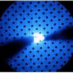
| The number of particles on a surface larger than 0.09 microns | 50 |
| Surface content of aluminium, E10AT/CM2 | 1 |
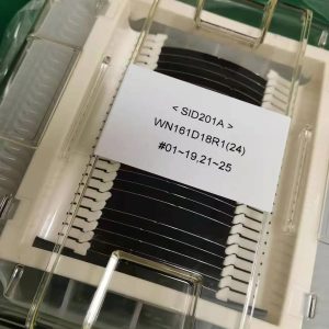
Packing requirements:
| Parameters | |
| Type of packaging | MW300GT-A |
| Inner Container Material | Polyethylene |
| Outer Packing Material | Aluminum |
| Number of pieces in one package | 25 |
| Reusability | yes |
2. Test Silicon Wafer Usage
Silicon wafers larger than 150mm are classified into Mechanical(dummy) Test Wafers and Process Test Wafers, and the test silicon wafer industry standards are in the following SEMI Standards(Semiconductor Equipment and Materials International, a global semiconductor association offered equipment, materials and service for manufacture of the worldwide semiconductor, photovoltaic (PV), LED, MEMS and flat panel display (FPD),and micro or nano-technologies).
3. About Silicon Wafer Test Grade
However, different application has required different parameters for mechanical or process test wafer:
Process Test Grade Silicon Wafers
Process Silicon Wafer Test Grade, is called Monitor wafer, which is for process monitoring and some processing applications in wafer fabrication. Wafer fab also use monitor test wafers to assess equipment cleanliness, support particle measurement or evaluate metallic contamination etc
Dummy Silicon Wafer
Dummy Silicon Wafer, also called Mechanical grade test wafer, is to test equipment for wafer dimensional and structural characteristics only, which is used to do equipment automation handling tests, reliability marathons, and software tests, and assess interoperability performance of wafer handling hardware.
Also silicon wafer fab use mechanical grade silicon test wafers to process development applications that are not sensitive for particle and defects.
Test Particle Grade Silicon Wafers
Test Particle Grade Silicon Wafers is for particle test monitors to measure wafer particle for applications, like CVD and ALD process.
According to SEMI standard, Particle of silicon wafer must be < 0.6 particles@>0.125μm/cm2 and < 0.15 particles@>0.25μm/cm2 for 250nm process and 130nm Design Rule Usage, 300mm wafers must have ≤60 LLS@>=90nm for 130nm process.
Silicon Wafers for Photolithography or Patterning Test
Test Silicon Wafers for Photolithography or Patterning Test mainly focus on requirement in wafer thickness variation, TTV, WARP, BOW and flatness. For instant, a 250nm wafer die Design, its corresponding SEMI Standard M24: Flatness per Site (SFSR) of ≤ 0.2μm at site size 25 x 25mm.
Furnace Grade Test Silicon Wafers
Furnace Grade Test Wafer Semiconductor has strictly requirement for electrical characteristics but not tight particle performance.
Resistivity of Furnace grade test silicon wafer should be above 1ohm.cm and doped very evenly with lifetime>=200us.
Also furnace grade wafers is strictly controlled oxygen and carbon content, as well as radial resistivity gradient.
Virgin Test Wafers
Virgin test silicon wafers are not used in semiconductor manufacturing, but for wafer process monitoring according to SEMI M8-93.
Solar Grade Silicon Wafer
Compared with IC grade silicon wafer, Solar Grade silicon wafer has lower requirement,
its purity is >=99.9999% while purity in IC grade is >=99999999,99%
4. FAQ:
Q: What is the Difference between Prime, Test and Dummy Silicon Wafer?
A: Prime grade silicon wafer is the best grade silicon wafer for formal wafer manufacturing and photolithography.
Test silicon wafer is the silicon wafer for equipment test or fab management and test.
Dummy grade silicon wafer is the silicon wafer for production process evaluation, or safety measure in production line.
Compared with Test grade silicon wafer, the parameters of dummy grade silicon wafer is much easier or loose for testing equipment for wafer dimensional and structural characteristics only. But it is not so strict to distinguish sometimes.