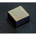

Test Wafer Monitor Wafer Dummy Wafer
As a dummy wafer manufacturer, UNIELECTRON offers silicone dummy wafer / test wafer / monitor wafer, which is used in a production device to improve safety in the beginning of production process and are used for delivery check and evaluation of process form. As dummy silicon wafers are often used for experiment and test, size and thickness thereof are important factors in most occasions. 100mm, 150mm, 200mm, or 300mm dummy wafer is available.
1. Test Wafer List
1.1 Single Side Polished Test Wafer N Type (200Nos)
| Sl No | Item | SCL SPECIFICATIONS |
| 1 | Growing method | CZ |
| 2 | Wafer Diameter | 150 ± 0.5mm |
| 3 | Wafer Thickness | 675±25 µm |
| 4 | Wafer Surface Orientation | <100>±2° |
| 5 | Dopant | Phosphorus |
| 6 | Dislocation Density | Less than 5000/cm2 |
| 8 | Resistivity | 4-7Ωcm |
| 9 | Radial Resistivity Variation (max.) | 15% |
| 10 | Flatness | |
| 10a | · BOW (max.) | 60 µm |
| 10b | · TIR (max.) | 6 µm |
| 10c | · TAPER (max.) | 12 µm |
| 10d | · WARP (max.) | 60 µm |
| 11 | Primary Flat | |
| 11a | · Length | 57.5±2.5 mm |
| 11b | · Orientation | {110}±2° as per SEMI Standard |
| 11c | Secondary Flat | As per SEMI Standard |
| 12 | Front Surface Finish | Mirror Polished |
| 13 | Max. particles of size ≥0.3µm | 30 |
| 14 | · Scratches, Haze, Edge Chips, Orange Peel & Other defects | Nil |
| 15 | Back Surface | Damage free Etched |
| 16 | Packing Requirement | Should be vacuum sealed in Class ’10’environment in double layer packing.Wafers should be shipped in Fluorware ORION TWO wafer shippers or equivalent make made from ultra clean polypropylene |
1.2 Double Side Polished Test Wafer N Type (150 Nos)
| Sl No | Item | SCL SPECIFICATIONS |
| 1 | Growing method | CZ |
| 2 | Wafer Diameter | 150 ± 0.5mm |
| 3 | Wafer Thickness | 675±25µm |
| 4 | Wafer Surface Orientation | <100>±2° |
| 5 | Dopant | Phosphorus |
| 6 | Dislocation Density | Less than 5000/cm2 |
| 8 | Resistivity | 4-7Ωcm |
| 9 | Radial Resistivity Variation (max.) | 15% |
| 10 | Flatness | |
| 10a | · BOW (max.) | 60 µm |
| 10b | · TIR (max.) | 6 µm |
| 10c | · TAPER (max.) | 12 µm |
| 10d | · WARP (max.) | 60 µm |
| 11 | Primary Flat | |
| 11a | · Length | 57.5±2.5 mm |
| 11b | · Orientation | {110}±2° as per SEMI Standard |
| 11c | Secondary Flat | As per SEMI Standard |
| 12 | Front Surface Finish | Mirror Polished |
| 13 | Max. particles of size ≥0.3µm | 30 |
| 14 | · Scratches, Haze, Edge Chips, | Nil |
| Orange Peel & Other defects | ||
| 15 | Back Surface | Mirror Polished |
| 16 | Packing Requirement | Should be vacuum sealed in Class ’10’ |
| environment in double layer packing. | ||
| Wafers should be shipped in Fluorware | ||
| ORION TWO wafer shippers or equivalent | ||
| make made from ultra clean polypropylene |
1.3 Monitor Wafer / Dummy Wafer
Monitor / Dummy Silicon wafer
| Wafer Diameter | Polished | Wafer Surface | Wafer Thickness | Resistivity | Particle |
| Orientation | |||||
| 4″ | 1 side | 100/111 | 250-500μm | 0-100 | 0.2μm≤qty30 |
| 6″ | 1 side | 100 | 500-675μm | 0-100 | 0.2μm≤qty30 |
| 8″ | 1 side | 100 | 600-750μm | 0-100 | 0.2μm≤qty30 |
| 12″ | 2 side | 100 | 650-775μm | 0-100 | 0.09μm≤qty100 |
1.4 REGENERATED 200mm WAFERS
| Item# | PARAMETER | Units | Value | Notes |
| 1 | Growth Method | CZ | ||
| 2 | Orientation | 1-0-0 | ||
| 3 | Resistivity | Ωм.см | 1-50 | |
| 4 | Type / dopant | р,n/ | ||
| Boron, Phosphorus | ||||
| 5 | Thickness | мкм | 1гр. – 620, | |
| 2гр. – 650 | ||||
| 3гр. – 680 | ||||
| 4гр. – 700 | ||||
| 5гр. – 720 | ||||
| 6 | GBIR (TTV | мкм | 1-3гр. <30, | |
| 4-5гр. <20 | ||||
| 7 | GLFR (TIR | мкм | <10 | |
| 8 | Warp | мкм | <60 | |
| 9 | Bow | мкм | <40 | |
| 10 | Metal contamination | 1/см2 | <3E10 | |
| 11 | Front surface | Polished | ||
| 12 | Front surface visual: | |||
| Haze, Scratches, Stains, Spots | none | |||
| Orange Peel | none | |||
| Cracks, Craters | none | |||
| 13 | Front Side LPD: | Number of wafers with stated parameter value should be not less than 80% of batch, | ||
| < 0,12мкм | <100 | |||
| <0,16мкм | <50 | |||
| <0,20мкм | <20 | |||
| <0,30мкм | <10 |
1.5 Coinroll Silicon Wafer
Spec : 12” , Bare Silicon, Thickness >750um , Notch , Slight scratch and stain that we will process IPA , DI water with Ultra sonic. (PAM171117-SI)
2. Dummy Wafer Definition
Dummy wafer (also called as test wafers) is a Si dummy wafer mainly used for experiment and test and being different from general wafers for product. Accordingly, reclaimed wafers are mostly applied as dummy grade wafers (test wafers).
In each process, film thickness, pressure resistance, reflection index and presence of pinball are measured using dummy Si wafer(test wafer). Also, dummy wafers (test wafers) are used for measurement of pattern size, check of defect and so on in lithography.
Monitor wafers are the bare silicon wafers to be used in the case that an adjustment is required in each production step prior to the actual IC production. For example, when the conditions of each process are set, such as the case of measuring tolerance of device against ( the variation of ) substrate thickness, coinroll silicon wafers for spacer wafers are being used as a substitution of high-standard and high value wafers. Moreover, they are also used for the monitoring purpose in the process together with product wafers. Monitor wafers are necessary wafer materials as important as product prime wafers. They are also called as test wafers together with dummy wafers.
For more product detail or if you have required specification, please contact us at [email protected] or [email protected].
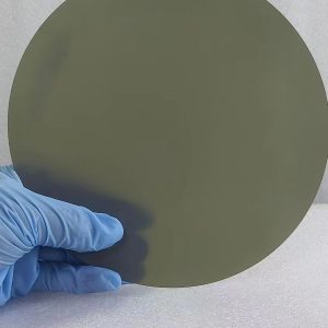
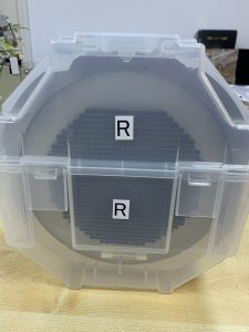
Test grade silicon wafers-1
Test grade silicon wafers-2
Test grade silicon wafers-3
Test grade silicon wafers-4
Test grade silicon wafers-5
Test grade silicon wafers-6
Test grade silicon wafers-7
Test grade silicon wafers-8
Test grade silicon wafers-9
Test grade silicon wafers-10
Test grade silicon wafers-11
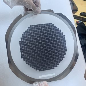
8″ Dummy Grade Silicon Wafer
12″ Dummy Grade Silicon Wafer Thickness 700-730um
12″ Dummy Grade Silicon Wafer Thickness 650-700um
12″ Test Grade Silicon Wafer
4″ Test Grade Silicon Wafers with Single Side Polished
12”Dummy wafer