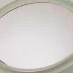

Epitaxial Silicon Wafer
Silicon Epitaxial Wafer(Epi Wafer) is a layer of epitaxial silicon single crystal deposited onto a single crystal silicon wafer(note: it is available to grow a layer of poly crystalline Silicon layer on top of a highly doped Singly crystalline silicon wafer, but it needs buffer layer (such as oxide or poly-Si) in between the bulk Si substrate and the top epitaxial silicon layer. It also can be used for thin film transistor.
The methods for preparing epitaxial silicon wafers include vapor phase epitaxy, liquid phase epitaxy, molecular beam epitaxy and so on. Among them, chemical vapor deposition (CVD)-based vapor phase epitaxy is the main silicon epitaxial growth process. Commonly used sources are SiCl4, SiHCl3, SiH2Cl2 and SiH4.
In order to meet the needs of various semiconductor devices, various silicon epitaxial technologies have been generated for epitaxial silicon wafer production. In addition to the silicon epitaxial growth in low temperature epitaxy and reduced pressure epitaxy, there is also selective epitaxy that deposits a silicon epitaxial layer on a specific part of the silicon wafer.
The epitaxial layer can be doped, as it is deposited, to the precise doping concentration while continuing the substrate’s crystalline structure.
Epilayer resistivity: <1 ohm-cm up to 150 ohm-cm
Epilayer thickness: < 1 um up to 150 um
Structure: N/N+, N-/N/N+, N/P/N+, N/N+/P-, N/P/P+, P/P+, P-/P/P+.
Wafer Application: Digital, Linear, Power, MOS, BiCMOS Devices.
Our advantages at a glance
1.Advanced epitaxial growth equipment, test equipment and epitaxial silicon technology.
2.Offer the highest quality with low defect density and good surface roughness.
3.Strong research team support and technology support for our customers
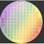
6″(150mm) Wafer specification:
| Item | Specification | |
| Substrate | Sub spec No. | |
| Ingot growth method | CZ | |
| Conductivity type | N | |
| Dopant | As | |
| Orientation | (100)±0.5° | |
| Resistivity | ≤0.005Ohm.cm | |
| RRG | ≤15% | |
| [Oi] Content | 8~18 ppma | |
| Diameter | 150±0.2 mm | |
| Primary Flat Length | 55~60 mm | |
| Primary Flat Location | {110}±1° | |
| Secondly Flat Length | semi | |
| Secondly Flat Location | semi | |
| Thickness | 625±15 um | |
| Backside Characteristics: | ||
| 1、BSD/Poly-Si(A) | 1.BSD | |
| 2、SIO2 | 2.LTO:5000±500 A | |
| 3、Edge Exclusion | 3.EE:?0.6 mm | |
| Laser Marking | NONE | |
| Front surface | Mirror polished | |
| Epi | Structure | N/N+ |
| Dopant | Phos | |
| Thickness | 3±0.2 um | |
| Thk.Uniformity | ≤5 % | |
| Measurement Position | Center(1 pt) 10mm from edge(4 pts @90 degrees) | |
| Calculation | [Tmax-Tmin]÷[[Tmax+Tmin]X 100% | |
| Resistivity | 2.5±0.2 Ohm.cm | |
| Res.Uniformity | ≤5 % | |
| Measurement Position | Center(1 pt) 10mm from edge(4 pts @90 degrees) | |
| Calculation | [Rmax-Rmin]÷[[Rmax+Rmin]X 100% | |
| Stack fault Density | ≤2(ea/cm2) | |
| Haze | NONE | |
| Scratches | NONE | |
| Craters、Orange Peel、 | NONE | |
| Edge Crown | ≤1/3 Epi thickness | |
| Slip(mm) | Total Length ≤ 1Dia | |
| Foreign Matter | NONE | |
| Back Surface Contamination | NONE | |
| Total Point Defects(particle) | ≤[email protected] |
Silicon Epi Wafers Sale-1
Silicon Epi Wafers Sale-2
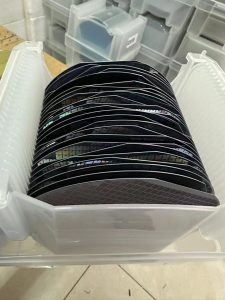
6″ Silicon EPI Wafer
4″ Silicon EPI Wafer-1
4″ Silicon EPI Wafer-2
4″ Silicon EPI Wafer-3
4″ Silicon EPI Wafer-4
4″ Silicon EPI Wafer-5
4″ Silicon EPI Wafer-6
3″ Silicon EPI Wafer-1
3″ Silicon EPI Wafer-2
3″ Silicon EPI Wafer-3
4″ Epitaxial Silicon Wafer
Silicon Epitaxy Growth with Boron Dopant by VPE
Epitaxy Wafer of Silicon for Integrated Waveguide Optics
P Type Boron Doped Silicon Epitaxial Wafer
Silicon PN Junction Wafer