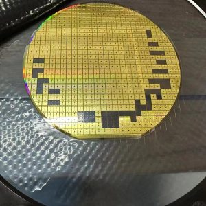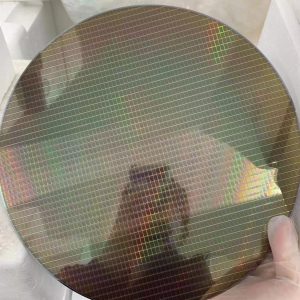

UNIELECTRON& SIC offer 300mm bare silicon wafers (12 inch) in prime grade, n type or p type, and the 300mm silicon wafer thickness is 775±15. Compared to other silicon wafer suppliers, Powerway Wafer’s silicon device wafer price is more competitive with higher quality. 300mm silicon wafers have a higher yield per wafer than pervious large diameter silicon wafers. Size on/above 8 inches (200 mm) is called a large silicon wafer. The production technology of large silicon wafer is not only the increase of process complexity because of the increase of area, but also the higher requirements on many other control factors. For example: oxygen content and its radial uniformity in wafer, impurity control, OISF control, etc. The silicon wafer requirements for defect control, oxygen precipitation control, resistance quantification, doping and radial uniformity are also higher. Especially for prime grade 300mm silicon wafer, some parameters are required critically, for instant, wafer TTV is below1.5um and defect density ~0/cm2. The next step is 450mm silicon ingot or wafer.
1. Parameters of 300mm Silicon Wafer
| Parameters | Value(PAM210512-300-SIL) |
| Type of ingot | Grown according to the Czochralski method |
| Diametr, mm | 300 ± 0,2 |
| Dopant | B (boron) |
| Conductivity type | P |
| Oxigen max, OLD-PPMA | 40 |
| Carbon , PPMA | 1 |
| Crystallographic orientation | <100> |
| Deviation from the predetermined surface orientation of crystal plane, deg | 1 |
| Volume resistivity, Ohm · cm | 8-12 |
| Primary Notch | Yes |
| Notch Location | 110 |
| Notch size, mm | 2,3 |
| Notch Form | V |
| Wafer thickness, microns | 775±15 |
| Type of marking | Laser |
| Marking Location | back side |
| Edge profile | by SEMI T/4 |
| Scratches on the front side | absent |
| Front side polishing | yes |
| Back side polishing | yes |
| Total change in wafer thickness (TTV), micrometers | 1,5 |
| Deflection (WARP), microns | 30 |
| The number of particles on a surface larger than 0.05 microns | 50 |
| The number of particles on a surface larger than 0.09 microns | 30 |
| Surface content of aluminium, E10AT/CM2 | 1 |
| Surface content of calcium, E10AT/CM2 | 1 |
| Surface content of chromium, E10AT/CM2 | 1 |
| Surface content of copper, E10AT/CM2 | 1 |
| Surface content of iron, E10AT/CM2 | 1 |
| Surface content of potassium, E10AT/CM2 | 1 |
| Surface content of natrium, E10AT/CM2 | 1 |
| Surface content of nickel, E10AT/CM2 | 1 |
| Surface content of zinc, E10AT/CM2 | 1 |
Packing requirements:
| Parameters | |
| Type of packaging | MW300GT-A |
| Inner Container Material | Polyethylene |
| Outer Packing Material | Aluminum |
| Number of pieces in one package | 25 |
| Reusability | Yes |
2. FAQ:
Q: Please take note that we offer “The number of particles on a surface larger than 0.09 microns 50” just for silicon substrate.
Normally the particle requirement is for silicon substrate.
To ensure the compliance, could you please check?
A: We double-checked: Yes, the indicated information is correct.