
UNIELECTRON can offer float zone silicon wafer, which is obtained by Float Zone method. Monocrystalline silicon rods is got through float zone growth, and then process the monocrystalline silicon rods into silicon wafers, called float zone silicon wafers. Since the zone-melted silicon wafer is not in contact with the quartz crucible during the floating zone silicon process, the silicon material is in a suspended state. Thereby, it is less polluted during the process of floating zone melting of silicon. The carbon content and oxygen content are lower, the impurities are less, and the resistivity is higher. It is suitable for the manufacture of power devices and certain high-voltage electronic devices.
1. Float zone silicon wafer specification
| ype | Conduction Type | Orientation | Diameter(mm) | Conductivity(Ω•cm) |
| High resistance | N&P | <100>&<111> | 76.2-200 | >1000 |
| NTD | N | <100>&<111> | 76.2-200 | 30-800 |
| CFZ | N&P | <100>&<111> | 76.2-200 | 1-50 |
| GD | N&P | <100>&<111> | 76.2-200 | 0.001-300 |
1.1 Floating zone silicon wafer specification
| Ingot Parameter | Item | Description |
| Growing method | FZ | |
| Orientation | <111> | |
| Off-orientation | 4±0.5 degree to the nearest <110> | |
| Type/Dopant | P/Boron | |
| Resistivity | 10-20 W.cm | |
| RRV | ≤15% (Max edge-Cen)/Cen |
1.2 FZ silicon wafer specification
| meter | Item | Description |
| Diameter | 150±0.5 mm | |
| Thickness | 675±15 um | |
| Primary Flat Length | 57.5±2.5 mm | |
| Primary Flat Orientation | <011>±1 degree | |
| Secondary Flat Length | None | |
| Secondary Flat Orientation | None | |
| TTV | ≤5 um | |
| Bow | ≤40 um | |
| Warp | ≤40 um | |
| Edge Profile | SEMI Standard | |
| Front Surface | Chemical-Mechenical Polishing | |
| LPD | ≥0.3 um@≤15 pcs | |
| Back Surface | Acid Etched | |
| Edge Chips | None | |
| Package | Vacuum Packing; Inner Plastic, Outer Aluminum |
2. Float-zone mono-crystalline silicon classifications
2.1 FZ-Silicon
The mono-crystalline silicon with the characteristics of low foreign-material content, low defect density and perfect crystal structure is produced with the float zone silicon process; no foreign material is introduced during the float zone silicon crystal growth. The FZ-Silicon conductivity is usually above 1000 Ω-cm, and such a high resistivity float zone silicon is mainly used to produce the high inverse-voltage elements and photoelectronic devices. It also can be used for dry etching process.
2.2 NTDFZ-Silicon
The mono-crystalline silicon with high-resistivity and uniformity can be achieved by neutron irradiation of FZ-silicon, to ensure the yield and uniformity of produced elements, and is mainly used to produce the silicon rectifier (SR), silicon control (SCR), giant transistor (GTR), gate-turn-off thyristor (GTO), static induction thyristor (SITH), insulate-gate bipolar transistor (IGBT), extra HV diode (PIN), smart power and power IC, etc; it is the main functional material for various frequency converters, rectifiers, large-power control elements, new power electronic devices, detectors, sensors, photoelectronic devices and special power devices.
FZ NTD Silicon Wafer with a Uniform Doping Concentration
2.3 GDFZ-Silicon
Utilizing the foreign-material diffusion mechanism, add the gas-phase foreign-material during the floating zone monocrystalline silicon process, to solve the doping problem of float-zone process from the root, and to get the GDFZ-silicon which is N-type or P-type, has the resistivity 0.001-300 Ω.cm, relative good resistivity uniformity and neutron irradiation. It is applicable for producing various semi-conductor power elements, insulate-gate bipolar transistor (IGBT) and high-efficiency solar cell, etc.
2.4 CFZ-Silicon
The monocrystalline-silicon is produced with the combination of Czochralski and float-zone processes, and has the quality between the CZ monocrystalline silicon and FZ monocrystalline silicon; the special elements can be doped, such as the Ga, Ge and others. The new-generation CFZ silicon solar wafers are better than various silicon wafers in global PV industry on each performance index; the conversion efficiency of solar panel is up to 24-26%. The products are mainly applied in the high-efficiency solar batteries with the special structure, back-contact, HIT and other special processes, and more widely used in the LED, power elements, automobile, satellite and other various products and fields.
Our advantages at a glance
1.Advanced epitaxy growth equipment and test equipment.
2.Offer the highest quality with low defect density and good float zone silicon surface roughness.
3.Strong research team support and technology support for our customers
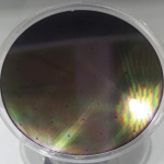
Si MEMS Wafer Grown by FZ
4″ FZ Prime Silicon Wafer
4″ FZ Prime Silicon Wafer
4″ FZ Prime Silicon Wafer-2
4″ FZ Prime Silicon Wafer-3
4″ FZ Prime Silicon Wafer-4
4″ FZ Prime Silicon Wafer-5
4″ FZ Prime Silicon Wafer-6
4″ FZ Prime Silicon Wafer-7
4″ FZ Prime Silicon Wafer-8
4″FZ Prime Silicon Wafer-9
2″ FZ Prime Silicon Wafer
3″ FZ Prime Silicon Wafer
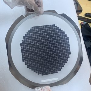
6″ FZ Prime Silicon Wafer
6″ FZ Prime Silicon Wafer
6″FZ Prime Silicon Wafer-1
6″FZ Prime Silicon Wafer-2
6″FZ Prime Silicon Wafer-3
5″ FZ Silicon wafers
6″ FZ Silicon Wafer
6″FZ Silicon Wafer-1
6″ FZ Silicon Wafer-4
6″ FZ Silicon Wafer-5
6″ FZ Silicon Wafer-6
6″ FZ Silicon Wafer-7
6″ FZ Silicon Wafer-8
8″ FZ Prime Silicon Wafer
3″ FZ Prime Silicon Wafer Thickness: 350±15um
4″ FZ Prime Silicon Wafer Thickness: 400µm +/-25µm
4″FZ Prime Silicon Wafer Thickness: 400µm +/-25µm-2
4″ FZ Silicon Ingot with Diameter 100.7±0.3mm
3″ FZ Silicon Wafer Thickness:229-249μm -1
3″ FZ Silicon Wafer Thickness:229-249μm -2
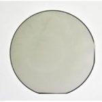
FZ Intrinsic undoped Silicon wafers
80+1mm FZ Si Ingot
80+1mm FZ Si Ingot-1
80+1mm FZ Si Ingot-2
80+1mm FZ Si Ingot-3
80+1mm FZ Si Ingot-4
80+1mm FZ Si Ingot-5
60+1mm FZ Si Ingot -1
60+1mm FZ Si Ingot -2
60+1mm FZ Si Ingot -3
60+1mm FZ Si Ingot -4
60+1mm FZ Si Ingot -5
60+1mm FZ Si Ingot -6
Silicon Block size 5x20mm
1″ FZ Silicon Ingot with Diameter 25mm
2″ FZ Silicon Ingot with Diameter 50mm
2″ FZ Si wafer with SSP
2″ FZ Intrinsic Silicon Wafer
2″ FZ Intrinsic Si Wafer SSP
2″ FZ Intrinsic Si Wafer DSP
4″ FZ Intrinsic Silicon Wafer SSP
4″ FZ Intrinsic Silicon Wafer DSP
4″ FZ Intrinsic Si wafer
4″ FZ N type Si wafer
3″ FZ Silicon Ingot with Diameter 76mm
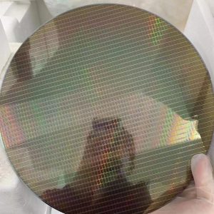
6″ FZ Silicon Wafer with Diameter 150mm, Both Side Etched
6″ FZ Silicon Ingot with Diameter 150.7±0.3mmØ