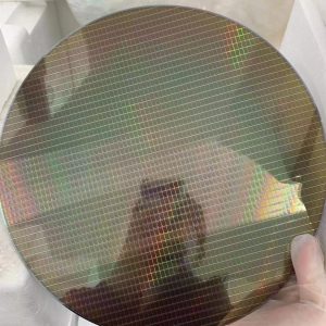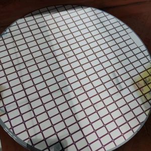


UNIELECTRON provides wafer foundry services in semiconductor manufacturing.
Thanks for advanced semiconductor process technology and benefit from our upstream experiences of substrate and wafer expaxy,
UNIELECTRON is to be the most advanced wafer technology and foundry services for fabless companies,IDMs and researchers.
Currently we have 200mm wafer fabrication facility (fab) for microfabrication.
Wafer Foundry Service
| Prozessname | Wafergröße (Zoll) | Fähigkeit |
| Schrittphotolithographie | 6 | 0,40 um |
| Kontaktierte Fotolithografie | 2,4 | 3um |
| Trockenätzen | 6 | Tiefe 100 um (Si),Metall, GaN |
| Nasse Bank | 6,8 | Metall, SiO 2, SiN, TEOS, Polysilicium |
| PECVD | 6 | SiN SiO2.TEOS |
| LPCVD | 6 | SiN, SiO2.Poly-Silizium |
| ALD | 6 | Al 2 O 3, AIN |
| Sputtern | 6 | Ti.Al, TiN, Ni, W. TiW.WN |
| Elektronenstrahl | 4,6,8 | Ti, Ni, Ag. Al.Ta, Cr Pt.Mo, Co. |
| Implantation | 6 | B (20 – 200 KeV, 1E13 – 115) .N |
| RTP | 6 | 900C max. |
| Backofen | 6 | 400C max. |
The foundry service capabilities for wafer fabrication are:
Metal Process for up to 8″ : Wafer metallization with Ti,Ni,Ag,Pt,Mo, Al, W,Cr, etc by sputter system or E-beam system
Dry Etch Process for up to 6″ by ALM,SAMCO RIE or ICP etching equipment
Film Process : SiO2, SiN, Al2O3 thin film by PECVD, DF&LPCVD, ALD and Unitemp RTP.
4.Lithography Process for 2″/4″/6″: Min. line width 0.4um by Nikon Stepper
Projection lithography: CD 2um, accuracy 1um
Ion implant equipment (B+, BF2 +, P+, As+, Ar+,B++, P++) for 2″/4″/6″ by ULVAC
Wafer fabrication process is done for processing raw wafers to finished chips.
Traditional wafer fabrication process involves individual steps for resistors, transistors, conductors,
and other electronic components processing on the semiconductor wafer.
We can offer Nanolithography (photolithography):Surface preparation, Photoresist apply, Soft bake,
Alignment, Exposure, Development, Hard bake, Develop inspect, Etch, Photoresist removal(strip), Final inspection.
Wafer Processing Service
Nanofabrication Service
For more information, please visit our website:https://www.powerwaywafer.com/wafer-fabrication
send us email at [email protected] and [email protected]